Introducing Lightning Arctic: Our latest In Situ TEM Cooling, Biasing & Heating solution

Introducing Lightning Arctic: Our latest In Situ TEM Cooling, Biasing & Heating solution

An interview with DENSsolutions Senior Product Manager Dr. Gin Pivak about our latest addition to the Lightning product family: Lightning Arctic.

DENSsolutions introduces its latest product: Lightning Arctic – an innovative in situ solution that can perform cooling, biasing and heating all in one system. In this article, we interview our Senior Product Manager Dr. Gin Pivak to learn all about Lightning Arctic, including its unique capabilities and wide application space.

1) What are the main application fields that will benefit from Lightning Arctic?

“There are numerous applications where Lightning Arctic can play an important role. The ability to cool a sample and apply electrical stimuli enables researchers to study low-temperature physics, reaching temperatures as low as 100 Kelvin. It can be utilized to investigate magnetic materials and nanostructures, superconductors, topological insulators, ferroelectrics and more. Additionally, the application of Lightning Arctic can be expanded to include beam-sensitive materials such as Li-ion batteries, organic superconductors and perovskite-based solar cells, where the cooling capability can prolong the material’s lifespan under the electron beam. Furthermore, the ability to perform electro and/or thermal experiments at high temperatures allows the Lightning Arctic system to be used in the fields of nanomaterials sintering and growth, metals and alloys, low-dimensional materials, resistive switching, phase-change materials, solid oxide fuel cells, piezoelectrics, solid-state batteries and so on.”

2) Has the system already been installed?

“Yes, the system has been installed at the Faculty of Engineering, Department of Materials at Imperial College London (ICL) in the UK. The main user of the Lightning Arctic system at ICL is Dr. Shelly Conroy, who is exploiting various ferroelectric and quantum materials at low temperatures and at atomic resolution.”

3) What are the main benefits of Lightning Arctic for users?

“Lightning Arctic brings forth numerous advantages for your in situ experiments:

1) Perform in situ cooling and heating experiments: A cooling rod inside the Lightning Arctic holder can transfer the ‘cold’ towards the tip of the holder where the MEMS-based Nano-Chip holding the sample is located. Once this cooling rod is connected to a detachable metallic cooling braid which is immersed in an external dewar filled with liquid nitrogen, the sample can be cooled inside the TEM down to liquid nitrogen temperatures. Aside from cooling, the Lightning Arctic holder also enables in situ heating experiments, where the temperature can reach 800 °C and even 1300 °C depending on the chip used.

2) Experience atomic imaging stability: The Lightning Arctic holder was uniquely designed to host a number of additional temperature controllers that work to stabilize the sample drift during cooling. One controller ensures the temperature equilibrium with the TEM while the other stabilizes the cold influx towards the sample. The usage of the external dewar that helps to minimize the liquid nitrogen bubbling ensures that atomic imaging with low sample drift can be achieved.

3) Continuous temperature control: Our state-of-the-art Heating and Biasing Nano-Chips enable the local manipulation of the temperature of the sample while not disturbing the cooling process of the holder. This means that you can achieve the fast setting of any user-defined temperature and the minimization of the image and focus shift when changing the temperature setpoint, all while ensuring atomic-scale imaging quality.

4) Achieve your required sample orientation: The double tilt Lightning Arctic holder allows tilting the sample in both alpha and beta directions of 10 – 25 degrees to find the required zone axis of the sample.

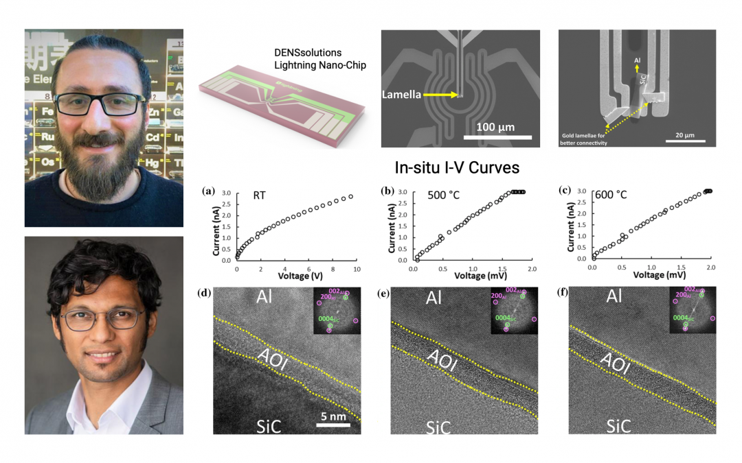
5) Perform in situ biasing experiments while cooling/heating: The Heating and Biasing Nano-Chips compatible with the Lightning Arctic holder contain biasing electrodes that can be used to apply and measure electrical signals either during cooling or during heating. Of course, the preparation of FIB lamellas on the Nano-Chips for electrical experiments is very crucial. There are already proven methods and tools developed for the Lightning system (like the DENSsolutions FIB stub) that can be used to prepare top-quality, short-circuit-free FIB lamellas on the Heating and Biasing chips for the Lightning Arctic system.

6) Wide compatibility of the sample carriers: Lightning Arctic has a similar Nano-Chip compatibility to the Lighting system, and works with Wildfire heating Nano-Chips and Lightning heating and biasing Nano-Chips. Moreover, the Lightning Arctic holder is also compatible with 3mm and lift-out TEM grids that can be used to study beam-sensitive materials at cryo-conditions without the need of using the Nano-Chips. This greatly expands the range of samples that the new in situ solution can work with.”


Read more about Lightning Arctic:


Download the Lightning Arctic brochure:

Subscribe to our newsletter to stay up-to-date with the latest in situ microscopy news.

DENSsolutions successfully installs both a Stream and Climate system at Cardiff University

DENSsolutions successfully installs both a Stream and Climate system at Cardiff University

From left to right: Oliver Mchugh and Dr. Thomas Slater from Cardiff University, Dr. Lars van der Wal and Alex Rozene from DENSsolutions

We are excited to announce that DENSsolutions has installed both a Stream and Climate system at the renowned Cardiff University in Wales, the United Kingdom. In this article, we interview Dr. Thomas Slater, Lecturer at Cardiff University, to learn more about the Cardiff Catalysis Institute Electron Microscope Facility, the team’s research direction and the pivotal role our Stream and Climate systems will play in advancing their research initiatives.

Can you tell me about the Cardiff Catalysis Institute Electron Microscope Facility?

“The Cardiff Catalysis Institute Electron Microscope Facility (CCI-EMF) is based at Cardiff University, one of Britain’s leading research Universities. The CCI-EMF is a new, world-class electron microscopy facility located in the University’s Translational Research Hub on its Innovation Campus. It houses an array of state-of-the-art imaging and analytical instruments designed around the study of heterogeneous catalysts and nano materials. The mission of the facility is to provide researchers in academia and industry with cutting-edge microscopy equipment, creating a Welsh hub for electron microscopy expertise and skills development.

In October 2022, we installed a 200 kV Thermo Fisher Scientific Cold-FEG Spectra 200. This aberration-corrected scanning transmission electron microscope (AC-STEM) is the first of its type in Wales. It is optimised for the study and analysis of heterogeneous catalysts and nanoparticles and is fitted with the Super-X EDS detector, Panther STEM detection system for HAADF/BF and iDPC imaging, Gatan’s Continuum ER EELS and Quantum Detectors Merlin detector. The facility also hosts a JEM-2100 LaB transmission electron microscope with a high-resolution Gatan digital camera and Oxford X-max EDS detector and a Tescan MAIA-3 field emission gun scanning electron microscope (FEG-SEM), which enables secondary electron (SE), in-beam SE, low-kV backscattered electron (BSE), in-beam BSE and scanning transmission electron microscopy (STEM) imaging capabilities.”

What type of applications are the users at CCI-EMF interested in using the Stream and Climate systems for?

“The Stream In Situ TEM Liquid + Biasing or Heating system will enable us to study liquid-phase reactions and follow the mechanisms of nanoparticle synthesis in solution. Nanoparticle growth and crystallization on the surface of metal oxide supports is of particular interest to us, along with catalyst stability in solution and the mechanisms of deactivation through leaching and particle migration.

The Climate In Situ TEM Gas + Heating system will allow the CCI researchers to conduct operando STEM, TEM and chemical imaging of heterogeneous catalysts under reaction conditions. We aim to develop an improved understanding of structure-activity relationships, oxidation and reduction processes, catalysts synthesis, catalyst stability and deactivation mechanisms. Crucially, we will be able to study changes in the structure and chemistry as a function of temperature, pressure and composition, improving our understanding of catalysed processes at or near real reaction conditions.”

What particular features of the DENSsolutions systems stood out to you?

“For us it was critical to have excellent thermal stability, a uniform heated zone and fast gas mixing at the cell to ensure reproducibility and correlation with our larger scale benchtop micro- reactors. Chemical compatibility with a wide range of reaction gases and catalyst materials was also important as we support a vast number of researchers across multiple research projects with very different experimental requirements.”

Could you tell us a bit more about the funding granted to acquire the systems?

“The system was purchased with European Regional Development Funding (ERDF) through the Welsh European Funding office (WEFO) and part-funded by The Wolfson Foundation. The funding enabled the CCI to establish its own EM facility through the purchase of advanced microscopes and equipment such as the DENSsolutions Stream and Climate systems. This capability enhances and strengthens the already outstanding catalyst research facilities of the CCI and our aim is to use this new capability to support the research needs of the University, our existing partners, local industry as well as develop new research strands.”

In your experience so far, how have you found working with Stream and Climate?

“The installation went very smoothly and was completed in a couple of weeks, including the 3 days of training. The hardware is robust, and the chip assembly relatively intuitive. We are able to have chips prepared, assembled, leak-checked and in the microscope within the space of a couple of hours which leaves the rest of the days free for experiments. The parameter control is made easy through the Impulse software workflow which guides you from start to finish. In fact, we were running experiments ourselves and generating data within a week of installation.”

Dr. Tom Slater
Lecturer |  Electron Microscopy of Catalytic Materials, Cardiff University

Dr. Tom Slater received his Ph.D. in Nanoscience from the University of Manchester, where he also did postdoctoral work in the Henry Moseley X-ray Imaging Facility. He then joined the electron Physical Sciences Imaging Centre (ePSIC) as an electron microscopy scientist. He was appointed as a Lecturer in Electron Microscopy of Catalytic Materials at Cardiff University in 2022, where his research focuses on imaging of heterogeneous catalysts.

Discover Dr. Slater’s publications:


Learn more about Stream:

Learn more about Climate:


Subscribe to our newsletter to stay up-to-date with the latest in situ microscopy news.

DENSsolutions forms new and exclusive partnership with Funa Scientific in China

DENSsolutions forms new and exclusive partnership with Funa Scientific in China

We are excited to announce that DENSsolutions has joined forces with Funa Scientific, our new dedicated distributor in China.

From left to right: Aaron Wan, Leo Li, Dan Zhou, Anton Qiu, Flora Cen, Simon Zhuang and Jerry Zhu

In the pursuit to strengthen and grow our business operations in China, DENSsolutions has partnered with Funa Scientific Co. – an established player in the electron microscopy industry. With this partnership, we plan to improve the speed and quality of our service and application support for our valued users in China. Moreover, we hope to make beneficial resources more accessible to local existing and potential customers, including user trainings, application support, webinars and publications. We are confident that this partnership will be fruitful for all parties involved, and most importantly for our customers. In this article, we introduce Funa Scientific so you can learn more about their services and values, as well as what to expect in the near future.

About Funa Scientific

Founded in 2012, Funa Scientific is a key provider of desktop scanning electron microscopes for universities, enterprises and research institutes. Importantly, they also help top overseas high-tech instrument manufacturers build a complete technical support and after-sales service system in the Chinese market, assisting users in scientific research innovation and problem-solving. At the very heart of the company is their customer-centric approach, whereby the innovation of products and the progress of the company are inseparable from the support of customers. Funa Scientific has an expansive customer base, including users from the most well-known enterprises and institutions around the world, accounting for 80% of the Fortune Global 500 companies, like Sony, Johnson Matthey, NASA and Siemens.

Funa Scientific conducts business in various regions of China, and each region has numerous sales engineers, application engineers and after-sales engineers. The company has testing centres and after-sales service centres in major cities across China, including Shanghai, Beijing, Guangzhou, and Chengdu.

Through long-term cooperation with key players in the microscopy industry to develop products such as the Thermo Fisher Scientific desktop scanning electron microscopes, VSParticle’s nano-research platform, Technoorg Linda’s Ar+ ion beam milling system and Forge Nano’s atomic layer deposition solutions, they have accumulated rich experience in the electron microscopy industry and nanoscale research technology. 

A bright future ahead

From this point onwards, Funa Scientific is the official distributor and business partner of DENssolutions in the Chinese market, fully responsible for the marketing, sales and service activities in China surrounding our solutions. Currently, Funa Scientific is working on setting up a dedicated local application research team and a Chinese website to be launched in the near future, which will feature the latest information about our advanced solutions and in situ microscopy news. Given Funa Scientific’s extensive expertise in the Chinese market, we are confident that this partnership will enable us to deliver our innovative solutions to a wider audience and better serve our customer base in China. We truly look forward to working closely with Funa Scientific to realize the bright future ahead.

Contact

If you have any questions for Funa Scientific, please reach out to their Product Director, Aaron Wan via email: aaron.wan@phenom-china.com or telephone: +8618516023887. Moreover, if you are based in China, we warmly encourage you to follow our WeChat account, run by Funa Scientific, so you can get all the latest updates. You can do so via this link or by scanning the following QR code. 

Subscribe to our newsletter to stay up-to-date with the latest in situ microscopy news.

DENSsolutions’ Lightning system helps uncover the interaction mechanism in reactive metal-ceramic system, Al-SiC

DENSsolutions’ Lightning system helps uncover the interaction mechanism in reactive metal-ceramic system, Al-SiC

Using the DENSsolutions Lightning system, researchers were able to provide an electrical, chemical and structural analysis of the Al–amorphous SiO₂–SiC interface at high temperatures.

Original article by Adabifiroozjaei et al.

The use of hybrid materials containing both metals and ceramics has become increasingly popular within manufacturing and microelectronic industries due to their optimized and well-balanced properties. Aluminum-silicon carbide (Al-SiC) is a widely known metal-ceramic composite material, commonly used in microelectronic packaging for automotive and aerospace applications. In Al-SiC an amorphous oxide layer (AOL) of SiO₂ is known to exist between the Al and SiC. Notably, the mechanism of interaction between the reactive metal (Al) and ceramic (SiC) and the AOL (SiO₂) under the heat-treatment process is still not well-understood. In fact, numerous theories about the interaction mechanism have been proposed over the past few decades. The major problem is that the studies conducted so far, regardless of the mechanism proposed in them, were ex situ and therefore not capable of resolving the atomic-scale nanostructural and chemical changes occurring at the interfaces during the heat-treatment process. In a recent paper published in the Journal of Materials Science, involving our valued users at TU Darmstadt, Dr. Esmaeil Adabifiroozjaei and Dr. Leopoldo Molina-Luna, the DENSsolutions Lightning system was utilized to reveal the evolution mechanism of the Al–AOL–SiC system under heating and biasing conditions. This study involved a team of researchers from institutes all over the world, including the University of Tabriz in Iran, NIMS and Shibaura Institute of Technology in Japan, and UNSW Sydney in Australia. 

Sample preparation

The first step for Dr. Adabifiroozjaei and his fellow collaborators was to carefully prepare the Al-SiC sample. After ultrasonically cleaning the SiC wafer, removing the oxide layer and allowing its regrowth by inserting the wafer into a desiccator, an Al layer with a thickness of ~1 µm was sputtered on the wafer using Shibaura’s CFS-4EP-LL sputtering machine. Next, in order to prepare the lamella, the researchers applied focused ion beam milling using JEOL’s JIB-4000 FIB. The prepared lamella was then loaded onto the DENSsolutions Lightning Nano-Chip (see Figure 1a). The low- and high-magnification scanning electron microscopy (SEM) images of the chip and the loaded lamella are shown below in Figure 1b) and 1c), respectively. Next, an Au lamella was prepared by FIB and connected to Al–AOL–SiC lamella and chip in order to ensure electrical current passes through Al–AOL–SiC lamella.

Figure 1: a) DENSsolutions Lightning Nano-Chip used for the in situ heating and biasing experiment, b) low- c) and high-magnification SEM images of the loaded lamella on the Nano-Chip, respectively.

Experimental results

The researchers performed EDX and EELS elemental mapping to determine the chemical composition of the phases across the Al–AOL–SiC interface. The EDS mapping of the interface is shown in Figure 2a), while the high-resolution EELS elemental mapping of the interface is shown in Figure 3b) – both of which reveal the consistent presence of a narrow oxide layer with a thickness in the range of 3–5 nm. 

Figure 2: a) EDS elemental mapping of Al–AOL–SiC interface, showing the presence of the AOL, b) STEM-HAADF image of Al–AOL–SiC interface and its EELS map profile.

Next, the researchers began with the in situ heating and biasing experiment to study the electrical characteristics of the lamella. First, a compliance current was set to 3 nA, then the voltage required to reach such a current was recorded at each temperature. The acquired I–V curves for room temperature, 500 ° and 600 °C after 30 minutes of application of the field are presented in Figure 3a–c), respectively. The I–V curves and high resolution TEM images (shown in Figure 3d–f) indicate that the resistivity of the Al–AOL–SiC device decreased three orders of magnitudes at 500 °C with no apparent change in the nanostructure. 

Figure 3: a), b), and c) show the I–V curves of Al–AOL–SiC interface measured at room temperature, 500° and 600 °C, respectively. d), e), and f) show the high-magnification images of Al–AOL–SiC interface from a small area of low-magnification images.

The chemical changes occurring at the interface during the heating process were investigated on another lamella using the same DENSsolutions Lightning holder, but on a Wildfire (heating-only) Nano-Chip. HAADF-STEM images and EELS chemical profiles were acquired and the results are shown in Figure 4 below. 

Figure 4: a), b), c ) and d) show changes in chemistry (line profiles of Al (Aqua), Si (Violet), C (Lime), and O (Yellow)) of Al–AOL–SiC interface at room temperature (25°), 550°, 500° and 600 °C, respectively.

During this analysis, the researchers observed that at 550 °C, the AOL width was reduced, which was specifically due to AOL dissolution into the Al. Moreover, the analysis of the structural changes at the interface nanostructure at 600 °C showed that the dissolution of the SiO₂ amorphous layer resulted in the formation of α-AlO and Si within the Al. In contrast, the elemental interdiffusion (Al³⁺ ⇄ Si⁴⁺) between Al and SiC was observed to occur, resulting in formation of AlC. From the results, we can infer that the reaction mechanism between Al and crystalline SiC is different with that between Al and SiO₂ amorphous phase.

Conclusion

Dr. Adabifiroozjaei and his fellow collaborators performed a comprehensive in situ STEM heating and biasing study using the DENSsolutions Lightning system, investigating the electrical, chemical and microstructural features of the interface of a Al–AOL–SiC system. Performing this study under an ultrahigh resolution of 4 Å allowed the researchers to confirm, for the first time in literature, that the reaction mechanism between reactive Al and crystalline SiC is different than between Al and amorphous SiO₂. Specifically, they found that whereas the reaction between SiO₂ and Al follows the dissolution mechanism, the reaction between SiC and Al proceeds through elemental interdiffusion. Importantly, these findings might be applicable to other reactive metal-ceramic systems that are currently used in manufacturing and electronic industries.

“With the stability and accuracy provided by DENSsolutions Lightning system, we could reveal features of an interfacial interaction in a common metal-ceramic system (Al-SiC) that were not previously observed. Such studies at very high resolution are absolutely necessary for the understanding and future development of composite materials at elevated temperatures.” 

Prof. Dr. Leopoldo Molina-Luna   Professor  |  TU Darmstadt

Original article:


Discover our Lightning solution:

Discover more publications made possible by Lightning:

Thomas article feature image

Liquid flow control: Unlock untapped research capabilities within in situ LPEM

Using the DENSsolutions Stream system, researchers were able to create a highly controlled chemical environment for visualizing the nanoscale metallic electrodeposition of copper crystals.

Subscribe to our newsletter to stay up-to-date with the latest in situ microscopy news.

DENSsolutions successfully installs another Climate system in Japan, at JFCC

DENSsolutions successfully installs another Climate system in Japan, at JFCC

Top row – from left to right: Mr. Suzuki (Nano Tech Solutions), Mr. Anada (JFCC), Dr. Lars van der Wal (DENSsolutions) and Mr. Hirai (JEOL). Bottom row – from left to right: Mr. Fukunaga (JEOL), Mr. Jinbo (JEOL) and Mr. Hisada (JEOL).

We are proud to announce that DENSsolutions has installed another Climate system in Japan, at the Japan Fine Ceramics Center, located in Nagoya, a highly populated Japanese port city. In this article, we interview Dr. Satoshi Anada, Senior Researcher at the Nanostructures Research Lab in JFCC, to learn more about their microscopy facility, its research direction, as well as how our Climate system is advancing their research.

Can you tell me about Japan Fine Ceramics Center and its research and development initiatives?

Japan Fine Ceramics Center (JFCC) was established back in 1985, with the goal of improving the quality of fine ceramics mainly through integrated testing and evaluation systems. JFCC has numerous business activities, one of which is the research and development (R&D) of materials, manufacturing technology and evaluation technology. Our R&D initiatives are focused on obtaining technological solutions to problems related to the environment, energy and safety. We have two main laboratories: 1) the Materials R&D Lab and 2) the Nanostructures Research Lab. The Materials R&D Lab focuses on the development of highly functional and novel materials (mainly ceramics) by improved process control, whereas the Nanostructures Research Lab focuses on the development and enhancement of state-of-the-art electron microscopy and related technologies. At the Nanostructures Research Lab, we have a high-end electron microscope – the JEOL JEM-ARM300F2 Grand ARM. This microscope enables us to observe samples at ultra-high spatial resolution with highly sensitive analysis over a wide range of accelerating voltages.”

What type of applications are the users at the Nanostructures Research Lab interested in using the Climate G+ system for?

“Users at the Nanostructures Research Lab are interested in applying the DENSsolutions Climate system to record operando TEM observations of battery and catalyst materials. We aim to understand where and how reactions take place, and which conditions enhance the performance of those materials. Moreover, we are interested in the electrochemical oxidation of materials in reaction with oxidants such as oxygen and hydrogen.”

What particular features of the DENSsolutions Climate G+ system attracted you to the system? 

“In order to understand factors and mechanisms related to the performance of battery and catalyst materials, it is important to observe their reactions in the actual environments in which they are used. The Climate system has the ability to flexibly and rapidly adjust gas composition, temperature, flow and pressure, which enables us to observe our battery and catalyst materials under various experimental conditions. This is capability is particularly what attracted us to the solution.”

In your experience so far, how have you found working with the Climate G+ system?

“The preliminary processes including the assembly of the Climate Nano-Reactor and leak testing are quite straightforward, assisted by the well-established Climate manual and software. With the Climate system, we have been able to perform numerous experiments without running into any leakage issues. Moreover, we are particularly impressed with the stability of the system even at extremely high temperatures.”

Dr. Satoshi Anada
Senior Researcher | Japan Fine Ceramics Center

Dr. Satoshi Anada received his Ph.D. degree in Engineering, Material Science, from Osaka University. Previously, he was working as a Specially Appointed Assistant Professor in the Research Center for Ultra-High Voltage Electron Microscopy at Osaka University. Currently, Dr. Anada is working as a Senior Researcher in the Japan Fine Ceramics Center (JFCC). His research was focused on the electromagnetic analysis of functional materials and devices using transmission electron microscopy, and now particularly on different microscopic measurement informatics.

Discover Dr. Anada’s publications:


Learn more about Climate:


Discover publications made possible by Climate:

Subscribe to our newsletter to stay up-to-date with the latest in situ microscopy news.