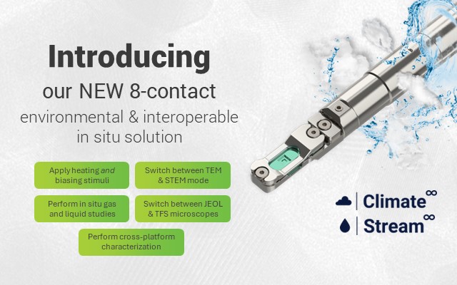
Introducing Infinity: DENSsolutions’ pioneering 8-contact environmental in situ solution
An interview with DENSsolutions’ Senior Mechanical Engineer about our latest innovation, Infinity – featuring an environmental holder with combined heating and biasing capabilities in both gas and liquid environments.

In this article, we delve into DENSsolutions’ cutting-edge Infinity solution through an exclusive interview with lead developer and Senior Mechanical Engineer, Christian Deen-van Rossum. Here, Christian takes us through the key features of this innovation, highlighting its benefits, diverse applications, and offering an inside look into the development journey of this advanced solution.
1) What are the main benefits of the Infinity solution for users?
“Climate Infinity and Stream Infinity bring forth numerous advantages for your in situ experiments:
1) Apply simultaneous heating and biasing stimuli: The new Climate/Stream Infinity holder features eight electrical contacts that enable simultaneous application of electrical and thermal stimuli in a gas or liquid environment. The contacts can be used for various electrically driven MEMS-based sensors and actuators, essentially transforming the Infinity system into a vast research playground. Importantly, for liquid studies, this opens the door to performing electrochemistry as a function of temperature.
2) Securely transfer your sample from one microscope to the other: The assembled tip of the Infinity holder containing a Nano-Reactor/Cell works as a cartridge, enabling complementary studies of the same sample using different TEM vendors, namely JEOL or Thermo Fisher Scientific (TFS). These microscopes can either be located in the same TEM lab, user facility or even in different universities/institutes. Remarkably, this removable tip also facilitates multi-modal characterization for SEM and beamline setups. Furthermore, the chips being used are universal, meaning that you can directly correlate experimental results obtained from JEOL and TFS microscopes, with improved Nano-Chip logistics.
3) Easily switch between STEM and TEM mode: By flipping the tip 180 degrees, you can directly change the sample position to be either on the top or bottom without a need to disassemble the tip. This grants you the freedom to flawlessly switch between STEM or TEM mode, respectively, depending on your experimental needs, while maintaining the best resolution performance. Importantly, you can switch between both imaging modes within a matter of seconds.
4) Perform gas and liquid studies with the same holder: The new environmental Infinity holder is your all-in-one solution for both gas and liquid experiments. Simply choose the appropriate function for the chips and connect the necessary gas or liquid supply system. Our extensive range of chip types includes gas-heating (GH), liquid-heating (LH), gas-heating-biasing (GHB), and liquid-heating-biasing (LHB), offering unparalleled versatility for your experimental needs. New MEMS chip designs will further expand the application space of the Infinity system.
5) Ease of use: We understand that a great product should be easy to use without a steep learning curve. Therefore, our design process focused on making sure the holder can be effortlessly utilized from the start. By prioritizing user-friendly design and continuously testing with real users, we ensured our product is not only powerful and effective but also simple and enjoyable to use. Because of this, the Infinity holder significantly reduces the time-to-experiment, allowing you to spend your time leveraging its capabilities to drive innovation and productivity. One highlight of the Infinity holder is the removal of all assembly tools and the introduction of self-aligning windows. When you place our chips in the tip of the holder, the membranes automatically align to provide a consistently clear field of view. Designed for a perfect fit, the Infinity holder ensures precise alignment without manual adjustments. This simplifies installation, reduces the risk of leaks, and allows you to focus more on your research and less on setup.
2) What inspired the development of Infinity, and what challenges did you encounter during the process?
“We wanted to bring a better, future-proof and more user-friendly holder to the market that truly meets the needs of our customers. For that reason we developed a holder from a customer-centric approach, driven by extensive customer input and thorough market research, rather than simply pushing the latest technology. We engaged with our customers to understand their challenges and desires and gathered invaluable feedback that helped shape every aspect of our product. By doing this we made sure that we were addressing real pain points and delivering solutions that would help improve the customer experience and reduce time to experiment. This customer-focused approach means that our product is not just a collection of the latest technological advancements, but a thoughtfully designed solution that reflects the actual needs and desires of our users.”
3) What are the main application fields that will benefit from Climate Infinity and Stream Infinity?
“The Infinity system can be used for broad applications ranging from materials science to energy and life science. In materials science, the Infinity system enables the study of nucleation, growth, assembly and corrosion under well-defined chemical environments (gas, vapor and liquid) and external stimuli (heating, biasing or both). The information obtained not only provides insights into the dynamic processes of material formation but also offers guidelines for the controllable synthesis of materials with improved performance. In energy studies, the Infinity system can mimic the real working conditions of various functional devices (such as batteries, supercapacitors, fuel cells, memristors, resistive random access memory, etc.). This allows the direct monitoring of the evolution and degradation of key materials, including rechargeable battery electrodes, thermo-, electro- and thermoelectro-catalysts and phase-change materials, at the nano- or even atomic scale. For life science, it is possible to image whole cells and resolve fine structures of biomaterials and proteins in their native state, and study various dynamics of biological samples in an environment close to a real organism. Moreover, the Infinity system provides a unique platform for correlative studies across different detection sources, such as electron, X-ray, neutron and visible light.”
4) Has Infinity already been installed?
“Yes, the system has been installed at numerous sites already, including EMAT (Antwerpen, Belgium), FAU Erlangen-Nurnberg (Erlangen, Germany) and UC Irvine (Irvine, USA).”
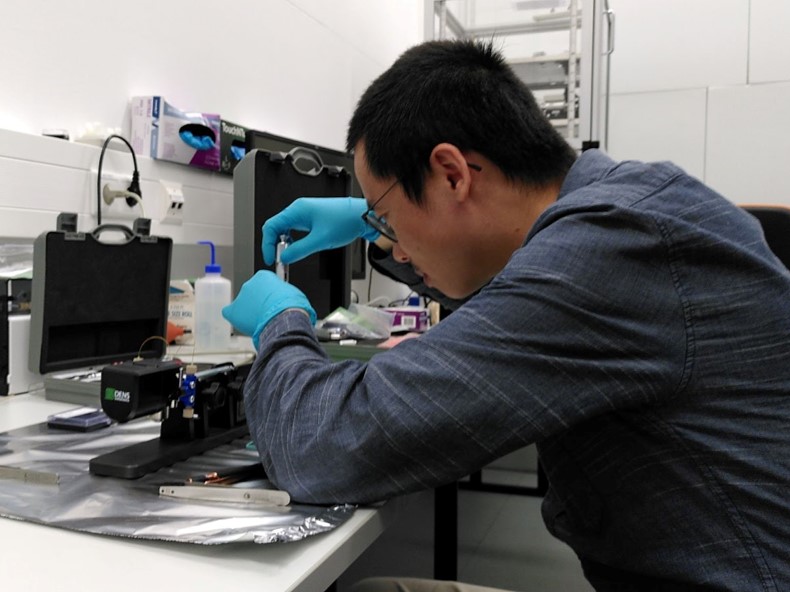
Dr. Mingjian Wu from FAU Erlangen-Nürnberg
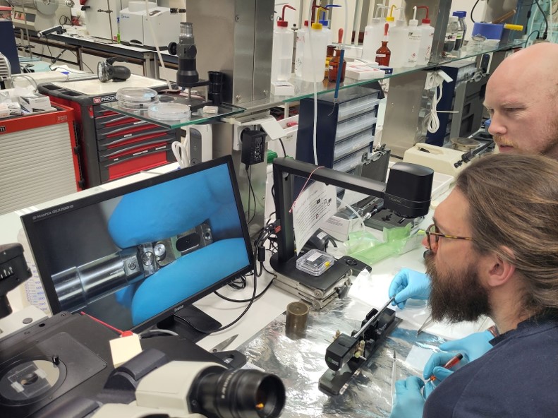
From left to right: Dr. Alexander Zintler from EMAT and Christian Deen van Rossum from DENSsolutions
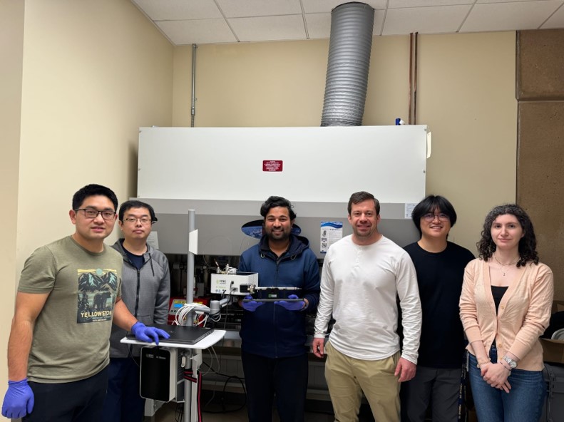
From left to right: Dr. Hongkui Zheng and Dr. Hongyu Sun from DENssolutions, as well as Pushp Raj Prasad, Prof. Joe Patterson, Zhaoxu Li and Elmira Baghdadi from UC Irvine
Dr. Mingjian Wu from FAU Erlangen-Nürnberg
From left to right: Dr. Alexander Zintler from EMAT and Christian Deen van Rossum from DENSsolutions
From left to right: Dr. Hongkui Zheng and Dr. Hongyu Sun from DENssolutions, as well as Pushp Raj Prasad, Prof. Joe Patterson, Zhaoxu Li and Elmira Baghdadi from UC Irvine
Read more about Climate Infinity:
Read more about Stream Infinity: