Scientists develop a novel approach to generate extreme thermal gradients using our Wildfire Nano-Chip

Scientists develop a novel approach to generate extreme thermal gradients using our Wildfire Nano-Chip

Via a simple modification to our Wildfire Nano-Chip, scientists show that extreme thermal gradients across a TEM specimen can be generated.

Original article by Sriram Vijayan, Rongxuan Wang, Zhenyu Kong and Joerg R. Jinschek

Marc Willinger TOC 1200x628

In traditional manufacturing processes, it is typically observed that the material experiences steady-state conditions. This results in the formation of stable equilibrium phases in the material. However, for those phases in materials that develop under ‘far-from equilibrium’ conditions, the same does not apply. In fact, for certain processing techniques that involve rapid thermal cycling and/or extreme thermal gradients, changes in the local phase equilibria, and therefore the local microstructure, often occur. Currently, observing these dynamic processes in materials under such conditions remains a great challenge. This is particularly because MEMS-based in situ TEM heating devices that can generate thermal gradients, combined with the capability to thermally cycle a specimen between different temperatures, are not currently available.

In recent research performed at The Ohio State University by Dr. Sriram Vijayan and Dr. Joerg Jinschek (now at Technical University of Denmark), as well as Rongxuan Wang and Dr. Zhenyu Kong from Virginia Tech, it is shown that controlled thermal gradients across a TEM specimen can be generated via a simple modification to our Wildfire Nano-Chip. Such a device can dramatically improve our understanding of material performance under extreme thermal conditions. Until now, thermally activated processes that affect microstructural stability of a material exposed to such thermal transients could only be investigated postmortem. Therefore, the need for new approaches to study thermally activated phenomena in materials in real time under such conditions is required. Importantly, this work is a major step forward in paving the way for scientists to be able to perform site-selective studies on materials under transient thermal conditions.

The study

As a first step, Dr. Vijayan and his fellow collaborators made modifications to a standard DENSsolutions Wildfire Nano-Chip. They then measured the local temperature distribution across the modified Nano-Chip and sample, and thereby the thermal gradient. The magnitude of the thermal gradient generated by this modified MEMS-based microheater was determined by measuring the temperature distribution using a combination of ex situ and in situ temperature measurement techniques. Regarding the ex situ temperature calibration, Dr. Vijayan and Dr. Jinschek teamed up with their MURI partners at Virginia Tech. As for the in situ temperature calibration, this was done at CEMAS, the state-of-the-art electron microscopy facility at The Ohio State University, using the previously established ‘Ag nanocube sublimation method’. 

The Nano-Chip modification

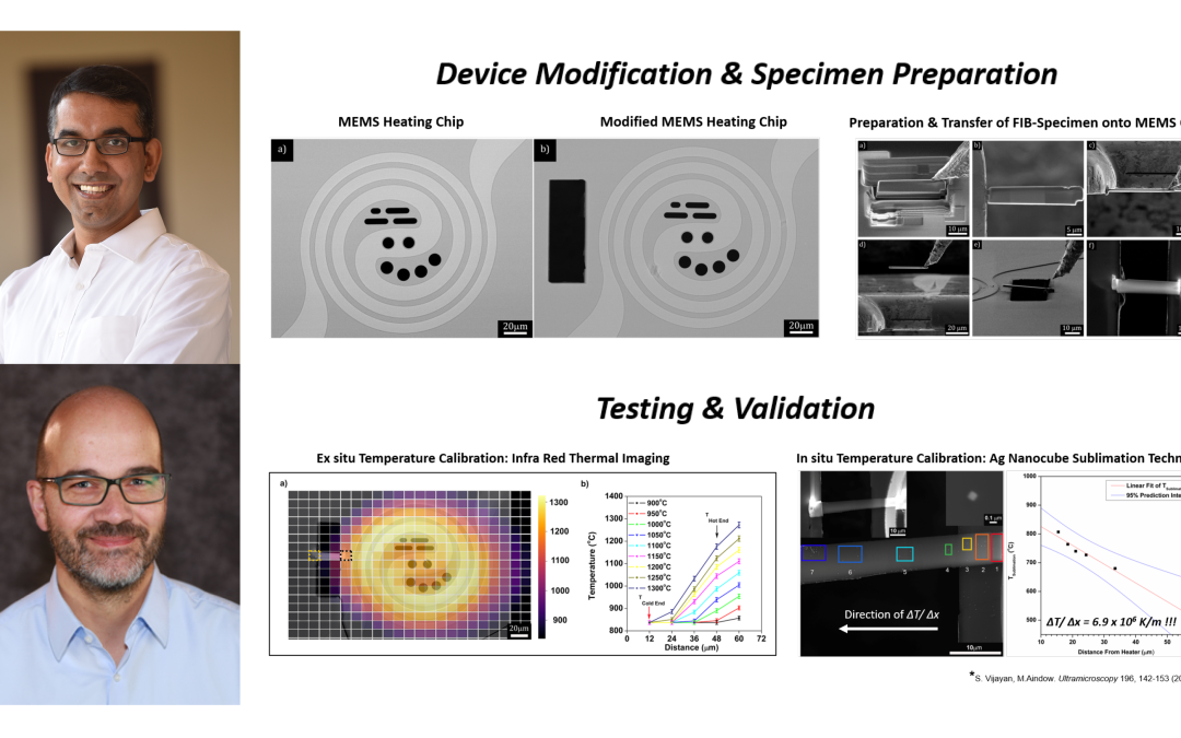
Using a Helios Nanolab 600 DualBeam focused ion beam (FIB)/scanning electron microscope (SEM), the researchers were able to modify a standard Nano-Chip. The Ga+ ion-based FIB was operated at an accelerating voltage of 30 kV and 6.4 nA beam current to mill a rectangular window next to the spiral metallic heater. This milled window can be seen in Figure 1b below. Importantly, after the FIB modification, the modified Nano-Chip exhibited no signs of deterioration in performance. 

Figure 2: Marc Willinger

Figure 1: SEM images of the (a) unmodified Nano-Chip and (b) modified Nano-Chip.

Lamella preparation and transfer

Next, the researchers worked on preparing and transferring the FIB lamella from a (001) oriented single crystal silicon wafer surface onto the Nano-Chip. This workflow is detailed in Figure 2a–f below. The FIB-cut Si lamella was placed across the larger window (Figure 2e), with one end of the lamella on the heater and the other end on the SiN membrane acting as the heat sink. The Si lamella was welded to the MEMS heater using a Pt-based Gas Injection System (GIS) needle with the aid of the Ga ion beam. The Pt was welded at the top left edge and top right edge of the lamella as seen from the SE Image in Figure 2f.

Figure 2: Marc Willinger

Figure 2: Secondary electron (SE) and ion (SI) images of the FIB preparation and transfer of the lamella over the modified window in the FIB.

Ex situ temperature calibration

At Dr. Kong’s lab (Virginia Tech), the researchers then performed infrared thermal imaging (IRTI) experiments on the MEMS devices under ambient air conditions. IRTI is a particularly useful ex situ approach to measure the spatial distribution of temperature across the MEMS-device with a reasonable degree of accuracy. Using IRTI, the temperature distribution was measured across both the unmodified and modified Nano-Chip. 

1) Temperature distribution across the unmodified Nano-Chip

First, the researchers measured the temperature distribution across the unmodified Nano-Chip to obtain reference temperature measurements. This distribution indicated that the metallic spiral heating element surrounding the viewing area of the microheater exhibited the highest temperature. Moreover, based on the temperature profile of the MEMS microheater, the spiral metallic heating element is the “hottest” region, while the surrounding SiN membrane is the “coldest” region on the MEMS device. These thermal conditions result in a large thermal gradient between the spiral metallic heater (= the “heat source”) and the SiN membrane (= the “heat sink”). 

2) Temperature distribution across the modified Nano-Chip

In order to generate a thermal gradient across a specimen, a FIB-cut lamella must be placed such that one end of the specimen is on or adjacent to the heater and the other end is on the SiN membrane, away from the heater. 

The researchers then performed IRTI again, but on the modified Nano-Chip with a FIB-cut lamella of Si placed across the modified window. As shown in Figure 3a below, the “hot end” of the Si lamella was adjacent to the outer spiral of the metallic heater, represented by the region enclosed in the black dotted square. On the other hand, the “cold end” was across the window in the SiN membrane, represented by the region enclosed in the yellow dotted square. Next, the thermal gradients across the FIB-cut TEM specimen were measured via an established technique that allows temperature measurement inside the TEM with high spatial resolution. 

Figure 2: Marc Willinger

Figure 3: Overlay of the SEM image of the modified device with Si lamella on the thermal map of the device at 1300°C (unit of heatmap scale is in C), (b) the horizontal temperature line profile along the “hot end” (enclosed in dotted black square) and “cold end” (enclosed in dotted yellow square) of the Si lamella.

In situ temperature calibration

In order to validate the ex situ results and accurately measure the temperature across the FIB-cut specimen, the researchers measured the temperature via the established Ag nanocube (NC) sublimation method. The lamella was again placed such that the “hot end” was over the central spiral metallic heater and the “cold end” across the modified window. Next, monodispersed Ag NCs were dispersed onto the FIB lamella. The modified Nano-Chip was then heated to a set point temperature of 1,000°C and held until the Ag NCs completely sublimate. In Figure 4a below, the Ag NCs that dispersed across the FIB lamella are highlighted with colored boxes and labeled as regions 1–7. After sufficient sublimation events on the lamella were observed, the sublimation experiment was halted. Notably, the Ag NCs in region 6 and 7 did not completely sublimate, as the sublimation kinetics slowed down at lower temperatures. 

“When exposing the FIB-cut TEM lamella to a combination of extreme thermal gradient heating and thermal cycling, the DENSsolutions Nano-Chip was observed to be extremely stable. The impulse software was very useful for these experiments as it allowed us to design complex temperature profiles during the heating experiments.” – Dr. Sriram Vijayan, Post-Doctoral Researcher, Center for Electron Microscopy & Analysis (CEMAS), The Ohio State University

The researchers then estimated the mean temperature of the Ag NCs on the FIB lamella found within regions 1–5. Subsequently, the mean temperatures obtained from regions 1 to 5 were plotted against the relative distance from the heater. In figure 4b below, a linear fit of the temperature data with 95% prediction intervals is presented. The thermal gradient of ΔT/Δx = 6.3 x 10⁶ °C/m was calculated at the temperature set point of 1,000°C. 

The in situ results confirm that the researchers’ proposed modification of our Wildfire Nano-Chip has indeed generated a large thermal gradient across the FIB-cut TEM specimen. In fact, this resulting thermal gradient was found to be in the range of gradients observed in several engineering and manufacturing applications. Ultimately, this innovative approach now opens up the scope of research to address a wide range of material science problems observed under transient thermal conditions.

Figure 2: Marc Willinger

Figure 4: (a) SEM image of different regions (1–7) across the Si lamella where the temperature of the lamella was measured. (b) The linear fit of the temperature from the “hot end” to the “cold end” superimposed over the plot of the measured sublimation temp from region 1 to 5 versus distance from the “hot end”.
.

Conclusion

This paper presents a very simple methodology to study non-equilibrium processes in materials under extreme thermal gradients and rapid thermal cycling conditions. Specifically, this modified Nano-Chip can enable dynamic studies of the microstructural evolution in materials used in several critical applications, including nuclear reactor components, microelectronic packages and additively manufactured builds. 

In the case of metal-based additive manufacturing (AM), extreme spatial and temporal thermal transients significantly impact the material microstructure within the melt pool and regions below the melt pool (‘previously melted’ layers of an AM build). Using this novel in situ TEM heating approach, we can now begin to observe and understand physical processes that contribute to the microstructural evolution in ‘previously melted’ layers during AM, thereby closing gaps in our understanding of processing-structure-property relationships in metal-based AM.

Ultimately, this powerful device can accurately simulate these complex thermal conditions inside the TEM and capture the microstructural evolution of materials during such extreme processing conditions. We are truly proud of the role that our Wildfire system has played in making this research possible and strive to continue enabling groundbreaking research now and in the future.

Hanglong Wu portrait

“Our modified DENSsolutions Wildfire Nano-Chip is well-suited for in-situ TEM heating experiments that require ‘far-from-equilibrium’ thermal conditions. This enables the observation of dynamic processes in a wide range of material systems at the nanoscale, which will further our fundamental understanding on microstructural stability of materials during processing and under ‘in-service’ conditions.” 

Dr. Joerg Jinschek
Professor |  Technical University of Denmark

Original article:

Discover our Wildfire solution:

Discover more publications made possible by Wildfire:

Thomas article feature image

New measuring technique proves exceptional temperature accuracy of our Wildfire Nanochip

In collaboration with Utrecht University, we develop a novel technique to measure temperature at the nanoscale, showing the remarkable temperature accuracy and homogeneity of our Wildfire Nanochip.

Subscribe to our newsletter to stay up-to-date with the latest in situ microscopy news.

New measuring technique proves exceptional temperature accuracy of our Wildfire Nanochip

New measuring technique proves exceptional temperature accuracy of our Wildfire Nanochip

In collaboration with Utrecht University, we develop a novel technique to measure temperature at the nanoscale, showing the remarkable temperature accuracy and homogeneity of our Wildfire Nanochip

Original article by Thomas P. van Swieten, Tijn van Omme, Dave J. van den Heuvel, Sander J.W. Vonk, Ronald G. Spruit, Florian Meirer, Hugo Pérez Garza , Bert M. Weckhuysen, Andries Meijerink, Freddy T. Rabouw and Robin G. Geitenbeek
Thomas article feature image

The temperature-sensitive luminescence of nanoparticles enables their application as remote thermometers. In fact, the size of these nanothermometers makes them ideal to map temperatures with a high spatial resolution. Yet, conducting high spatial resolution mapping of temperatures that exceed 100°C poses some challenges.

In collaboration with Thomas van Swieten and his fellow colleagues at Utrecht University, we were able to jointly develop a new technique to measure temperature at the nanoscale. In fact, we tested this novel technique on our Wildfire Nanochip and were able to further confirm the Nanochip’s unparalleled temperature accuracy and homogeneity. These experiments also proved how well our models work to predict the temperature distribution across the microheater. Importantly, this particular technique will improve the accuracy of nanothermometry as a whole, not only in micro- and nano-electronics but also in other fields with photonically inhomogeneous substrates.  

The technique: Luminescence nanothermometry

Thermometry on the microscopic scale is an essential characterization tool for the development of nano- and microelectronic devices. However, conventional thermometers like thermocouples are often unable to reliably measure the temperature on this length scale due to their size. This is precisely where remote temperature sensing via optical thermometry techniques comes into play. Thermometry based on luminescence is particularly interesting since it is easily implemented, requiring only the deposition of a luminescent material in or on a sample of interest and the detection of its luminescence. For this reason, luminescence nanothermometry is currently developing into the method of choice for temperature measurements in microscopy.

Homogeneous heat distribution

Our Wildfire Nanochip was specifically designed to enable users a homogeneous heat distribution across the microheater where a sample is positioned. It is particularly due to the unique geometry of the metal spiral, where the windows are placed right at the center, that users are able to enjoy such a remarkable temperature homogeneity. In fact, our Wildfire Nanochip has a temperature uniformity of 98% across the window area and 99.5% across the two central windows. The figure on the right below is a perfect illustration of the chip’s exceptional temperature homogeneity, showing the temperature profile across the membrane and the microheater for a center temperature of 523 K simulated with a finite element model.

The high temperature homogeneity of our Wildfire Nanochips is also owed to the fact that the metal heating spiral is embedded in a silicon nitride membrane. Silicon nitride has many advantages including being chemically inert, mechanically robust and can withstand harsh chemical and temperature environments. 

Tijn article - figure 2 wildfire nanochip homogeneous distribution

On the left: The Wildfire Nanochip, where the metal spiral is represented in orange and the silicon nitride membrane in blue. On the right: Finite element model simulation showing the remarkable temperature homogeneity of the Wildfire Nanochip

Reliable temperature mapping

In this work, the luminescent particles that were used are NaYF₄ nanoparticles doped with Er³⁺ and Yb³⁺. These particles exhibit a strong upconversion when excited with an infrared laser. In other words, they emit photons with a shorter wavelength than the excitation photons. As shown in the figure below, we found that the spectrum of the emitted (green) photons is quite sensitive to temperature.

Tijn article - Figure 1 Intensity vs Wavelength

Green upconversion luminescence of the nanoparticles upon excitation at various temperatures ranging from 303 K (dark red) to 573 K (yellow)

By scanning the laser across a layer of deposited nanoparticles in the confocal microscope, we were able to capture an array of emission spectra. We then converted this emission spectra into a temperature map using the luminescence intensity ratio of the 2 peaks at each pixel. After a number of correction steps, the technique showed a remarkable precision of 1-4 K with a spatial resolution of ∼1 micrometer. It is noteworthy to mention that most other techniques are unable to achieve such a high accuracy like this.

Tijn article - Figure 3 DESKTOP reliable temperature mapping

In a) we scanned the laser across the microheater with the deposited luminescent nanoparticles to generate a map of intensity ratios. b) shows the spectrum at each pixel converted into a temperature to provide a temperature map of the microheater.

Simulation and model accuracy

Using the fully corrected temperature maps, we were able to analyze in depth the temperature homogeneity of the microheater. The figure below shows the horizontal traces through the center of these maps. The simulated temperature profiles (lines) show an excellent match with the experimental traces (dots).This confirms both the reliability of the finite element model as a design tool and the strength of our temperature mapping technique as a characterization tool, achieving a high accuracy and a spatial resolution of ∼1 μm.

Tijn article - temperature mapping in graph

A graph showing the mapping of elevated temperatures. The lines represent the simulated temperature profiles and the experimental traces represent the dots.

We determine the standard deviation of the temperature in the center to quantify the accuracy of this thermometry method and find values of 1 K at 323 K increasing to only 4 K at 513 K. Conclusively, this makes nanothermometry using confocal luminescence spectroscopy a promising method to map temperature profiles not only for microheaters but also in other fields such as biology and catalysis where temperature variations are important but hard to monitor with conventional methods.
Tijn portrait image
“Thanks to the exceptionally good spatial and temperature resolution of this method, we were able to obtain an accurate temperature map of our microheater spiral. This confirmed the excellent temperature homogeneity which was predicted by our finite element models.”
Tijn van Omme
Microsystems Engineer |  DENSsolutions

Original article:

Discover our Wildfire solution:

Discover more publications made possible by Wildfire:

Markus article feature image

The first in situ observation of layered metastable heterostructure formation

Using our Wildfire system, scientists are able to thoroughly investigate the formation of heterostructures from starting materials with vastly different properties

Do you want to receive great articles like this in your mailbox? Subscribe to our newsletter.

The first in situ observation of layered metastable heterostructure formation

The first in situ observation of layered metastable heterostructure formation

Using our Wildfire system, scientists are able to thoroughly investigate the formation of heterostructures from starting materials with vastly different properties

Original article by Markus Terker, Lars Nicolai, Samuel Gaucher, Jens Herfort and Achim Trampert

Markus Terker top image in article graph

A plot showing the STEM images taken of the heterostructure demonstrating a tendency for disordered layers to order over time with annealing

Heterostructures, semiconductor structures composed of solid-state materials with different chemical properties, have found use in a variety of specialized applications where their unique characteristics are critical. The engineering of heterostructures is an important means in creating novel device concepts. In fact, it has already revolutionized the development of solar cells, transistors and even lasers. However, layering materials with vastly differing properties poses complex challenges.

Using the DENSsolutions Wildfire system, Markus Terker and his colleagues from the Paul-Drude-Institut in Berlin, Germany observe for the first time the atomic formation of a layered, metastable iron germanium crystal via two-step phase transformation. This research opens doors towards the design and formation of novel hybrid materials that combine vastly different properties, such as ferromagnets and semiconductors, and has appealing implications for optical-electronic industries.

Heterostructural interfaces and stability

Heterostructural interfaces are fundamental and versatile tools when designing electronics with varying properties, such as magnetic, optical, and transport capabilities. Since these interfaces can be used to stabilize otherwise metastable structures, understanding their structures and formation is essential to harnessing the full potential of these materials. Shedding new light on the growth of these interfaces from disordered to ordered states opens up the potential for new applications of this technology.

In this research, Terker and his colleagues observed the in situ annealing of two materials and the resulting FeGe₂ alloy interface between them. This gradual process, catalogued in the figure below, shows the crystallized FeGe₂ at the interface slowly ordering itself into layers of material.

Markus Terker figure 1 showing snap shots of annealing

In situ snapshots of the alloy interface ordering itself into periodic layers over the span of 60 minutes

From disorder to order

The starting sample consisted of a layer of Fe₃Si interfaced with amorphous germanium, a semiconductor. Heating the sample to 300 °C initiated the crystallization process and a thin layer of FeGe₂ crystal formed at the interface. This layer then grew as the sample was sustained at this temperature for the duration of an hour.

Whilst the sample was heated, in situ images were taken of the progression of the FeGe₂ crystal as it grew along the surface of the Fe₃Si base. After 15 minutes of annealing, the majority of the amorphous germanium film completely crystalized and reduced in size and disorder. However, this stage was still not completely ordered. By the 30-minute mark, the amorphous film completely crystalized and gradually ordered itself layer by layer until the entire film was in an ordered phase. 

STEM images of the (b) disordered and (c) vacancy-ordered structure of FeGe₂ observed. Atomic models of the (a) disordered and (d) ordered phase of FeGe₂ observed. The colored dots indicate the atomic stacking order.

Metastable structure

Although it was expected that pure germanium would form during this solid-phase epitaxy, the researchers observed something else entirely. A strong diffusion of iron into the germanium film was detected at relatively low crystallization temperatures. Moreover, instead of pure germanium with a diamond structure, an epitaxial film with iron content was obtained. High-angle annular dark-field (HAADF) scanning transmission electron microscopy (STEM) confirmed that the resulting crystal had a different metastable crystal structure to what was expected. The figure below shows the heterostructure produced after the annealing process. 

The heterostructure produced after the annealing process

STEM images taken of (a) the heterostructure produced after the annealing process, and (b) a magnified image of the dotted black box showing the vacant layers

Novelty in findings

Phase transformations are one of the most fascinating phenomena in nature. Observing such transformations in real time and with the resolution of individual atoms could revolutionize our understanding of their chemical and physical processes. This research demonstrates that a novel crystal phase of FeGe₂ can be interfaced from two materials with vastly different physical properties: Fe₃Si, a ferromagnet, interfaced with amorphous germanium, a semiconductor. Terker and his colleagues were able to demonstrate that a hybrid sample preparation approach can yield thin samples suitable for high resolution HAADF STEM while at the same time retaining the sample composition and structure. This approach could be applied to many different heterostructures and lead to a much broader applicability of the in situ TEM method in the study of phase transformations.

Markus personal image improved

“For the atomic scale investigation of small nanostructures at high temperatures, the reduction of sample drift is of paramount importance. The new generation of DENSsolutions Wildfire Nanochips offer the ideal solution for this due to their small and reproducible bulging. Their robustness also enables an easy and safe transfer of the specimen lamella of any form or sample geometry.”

Markus Terker
PhD Student |  Paul-Drude-Institut in Berlin, Germany 

Original article:


Discover our Wildfire solution:

Discover more publications made possible by Wildfire:

Torsten feature image

Visualizing the structural evolution of thermally-decaying platinum nanowires


Using our Wildfire system, scientists gain an exceptional in-depth understanding of the morphological changes of platinum nanowires at certain temperatures

Do you want to receive great articles like this in your mailbox? Subscribe to our newsletter.

Visualizing the structural evolution of thermally-decaying platinum nanowires

Visualizing the structural evolution of thermally-decaying platinum nanowires

Using our Wildfire system, scientists gain an exceptional in-depth understanding of the morphological changes of platinum nanowires at certain temperatures

Original article by Torsten Walbert, Falk Muench, Yangyiwei Yang, Ulrike Kunz, Bai-Xiang Xu, Wolfgang Ensinger, and Leopoldo Molina-Luna

Torsten feature image

The morphological transformation of a platinum nanowire as temperature increases and the two domain types observed

Metal nanowires represent a main class of one-dimensional nanomaterials and have been proven essential for a wide range of applications. Previous works on electrodeposited nanowires focused on ex situ SEM characterization, which is limited in terms of resolution and unable to monitor internal nanostructure changes. Using the DENSsolutions Wildfire system, Torsten Walbert and his colleagues from the Materials Analysis group and Prof. Leopoldo Molina-Luna from the Advanced Electron Microscopy (AEM) Division at the Institute for Materials Science, TU Darmstadt were able to investigate via in situ TEM the influence of temperature on polycrystalline platinum nanowires. Observing this process under remarkably high resolution enabled them to capture for the first time the internal transformations during both early and intermediate stages of the platinum nanowire decay. 

The structural evolution of nanowire decay 

Although nanowires are crucial for a wide range of applications, they are frequently prone to degradation. It is important that we understand these underlying failure mechanisms to better ensure reliable performance under operating conditions. Previous studies observing the thermal decay of nanowires have typically focused on ex situ investigations inside an SEM. Only a handful of studies look at the in situ characterization of nanowire decay using TEM, but even those focus specifically on gold nanowires. In this study, Torsten and his team observe the temperature influence on the degradation of platinum nanowires. Platinum is used due to its high mechanical, chemical and thermal stability as well as catalytic activity.

Below you can see an overview of the morphological transformation of a platinum nanowire after a thermal treatment between 250°C and 1100°C. It is observed that the main external transformation starts after 800°C, illustrated by the corresponding diameter evolution.

Structural evolution of pt nanowires

The morphological transformation of a platinum nanowire after thermal treatment and corresponding diameter evolution

Changes in internal nanostructure

Although external shape transformations occur after 800°C, changes in the internal nanostructure happen a lot earlier at markedly lower temperatures. As shown in the figure below, after heating to 250°C, no pronounced changes in the internal structure are observed compared to the initial state. After increasing the temperature to 450°C, the nanowire outline is still unaltered, but voids of low contrast (indicated by red circles) already start appearing. At 800°C, these voids begin to propagate and the shape slightly changes.

Further increasing the temperature to 850°C causes a grain boundary to extend, which is indicated by the dashed green line in the figure below. Finally, at 875°C, the grain boundary straightens while the voids increase and accumulate. Ultimately, these results confirm that internal nanowire restructuring considerably precedes the permanent changes of the outer nanowire shape. In fact, the observed faceted voids and grain boundaries are crucial factors guiding their transformation and final splitting, which is discussed in the next section.

TEM image showing the formation of voids (red circles) and straightening of grain boundary (green dashed line) at low and high temperatures

TEM video showing a void disappearing from a single-crystalline wire segment

Two surprising domain types

Some surprising results are observed after when the temperature goes beyond 875°C. Interestingly, the nanowires segregated into two domain types, one being single-crystalline and essentially void-free, while the other preserves void-pinned grain boundaries. This is the first time in academia that researchers observe this type of segregation, as it was neither described in previous experimental studies nor predicted by simulations.

You can see in the simulation and TEM video below that the wire separates into two domains, a single-crystalline domain and void-containing domain. Whereas the single-crystalline areas exhibit fast platinum transport, the void-containing areas show an unexpected morphological stability, retaining their nanostructure even at temperatures above 1000°C. In fact, the subsequent splitting of the nanowires is only observed in single-crystalline areas and thus leads to the formation of fragments with varying lengths and diameters. 

A simulation of the platinum nanowire disintegration, showing the curvature-driven mass transfer dominating the nanowire transformation

TEM video showing the disintegration of a platinum nanowire into two fragments

Novelty in findings

Performing in situ TEM in a controlled temperature environment represents a powerful approach for investigating the structural transformations of metal nanowires. Obtaining detailed insights into the internal nanostructure of nanowires and their evolution over time would otherwise be impossible without in situ TEM. Torsten and his team were able to relate the onset of shape changes to distinct nanostructural features acting as starting points in the disintegration process. This study is not only of great interest for basic research, but also helps in predicting the thermal robustness and reliability of nanowires in devices and can serve as a synthetic tool, enabling the control over the disintegration sequence via defect engineering. If we can understand the mechanism behind the process of decomposition, we can better predict and control the thermal stability of nanowires, adapting their shape and properties according to specific applications and conditions. 

Walbert, Torsten portrait -400 px

“The DENSsolutions Wildfire chip enabled an exact and fast temperature regulation with a homogeneous heat distribution, allowing us to investigate the decomposition process of Pt nanowires in situ. Without it, it would not have been possible to follow the transformations of the nanowires directly and to link them to the internal changes in the nanostructure.”


Torsten Walbert
PhD Student | Technische Universität Darmstadt

Original article:


Discover our Wildfire solution:

Discover more publications made possible by Wildfire:

Dental crown created by selective laser melting (SLM)

Improving the mechanical properties of 3D printed metal parts


Using our Wildfire system, researchers explore the microstructural changes occurring in AlSi10Mg during 3D printing and post processing

Do you want to receive great articles like this in your mailbox? Subscribe to our newsletter.

Improving the mechanical properties of 3D printed metal parts

Improving the mechanical properties of 3D printed metal parts

In situ TEM helps to understand the microstructural changes in AlSi10Mg during 3D printing and post processing

 
Original article by Mihaela Albu, Robert Krisper, Judith Lammer, Gerald Kothleitner, Jacopo Fiocchi and
Paola Bassani
Dental crown created by selective laser melting (SLM)

Dental crown created by selective laser melting (SLM)

Selective laser melting (SLM) is an additive manufacturing technique used to create unique products for the medical technique, automotive-, aeronautic- and space industry. AlSi10Mg alloy is widely used for this technique because of its low weight, corrosion resistance, good thermal properties, specific strength, and flexible post processing capabilities. The mechanical properties of 3D printed parts show better values compared to parts that are made using traditional casting of metal. But these values decrease after conventional heat treatment. In this research, scientists from Graz Centre for Electron Microscopy, Austria, tried to understand the fundamental mechanisms responsible for the drop in mechanical properties after heat treatment.
This work provides the first correlative in-situ heating multiscale analysis of the powder and the additive produced AlSi10Mg alloy, allowing a unique insight into material transitions at the micro-and nanoscale. The researchers showed that microstructural changes like crystallization of eventually present amorphous phases and the evolution of Si nanoparticles evenly dispersed in the Al-matrix are the most important factors that contribute to the enhancement or decrease of the mechanical properties.

Towards affordable 3D metal printing

Nowadays, selective laser melting (SLM) refers to the most common system used to create metal parts from powders as feedstock. Despite its popularity, powder based additive manufacturing is still an expensive process, and consequently, getting proof components at the first attempt is of great economic interest. Manufacturers of such parts strive for optimizing their processes, not only to improve material properties, but also to enhance the interchangeability of building platforms and thus, their economic flexibility. Controlling these production aspects and finding an adequate post-processing strategy helps to fine-tune the microstructural features, and therefore the mechanical properties, according to different application fields.

Low magnification HAADF STEM video 80°C to 360°C in 20°C steps for the as-built sample, maintaining the isothermal stages for 4 min each
Atomic resolution video of a Si nanoparticle in the Al-matrix during in-situ heating

Benefits of in situ STEM

In-situ heating experiments in scanning transmission electron microscopes (STEM) enable immediate information about the structural, morphological and chemical changes and are thus helpful for the selection of various post-processing strategies.

DENSsolutions Wildfire System TF FEI

The DENSsolutions Wildfire H +DT system enabled the fast heating and cooling that allowed us to perform nanoscale crystallographic and chemical analyses at certain temperatures that corresponded to the exothermic peaks in DSC measurements and to the in-situ XRD measurements.

Dr. Mihaela Albu
“In-situ heating experiments performed on 3D printed materials enable breakthrough advances in printing and post-process optimization. DENSsolutions Wildfire system proved to have superior thermal and spatial stability, ensuring high-resolution investigations at higher temperatures.”

Dr. Mihaela Albu
Senior Scientist | TEM at the Austrian Centre for Electron Microscopy and Nanoanalysis

Original article:

More about Wildfire:

Do you want to receive great articles like this in your mailbox? Subscribe to our newsletter.

EUSMI Nanostars Project

EUSMI Nanostars Project

Nothing could better illustrate the excellence of EUSMI Joint Research Activity (JRA), than the Nanostars project, which has combined the expertise of three EUSMI partners from three distinctive areas: CIC biomaGUNE, EMAT and DENSsolutions.

Nanoparticles are a versatile functional material and have much potential in medical applications. The chemists at CIC biomaGUNE have successfully synthesized a novel type of nanoparticles, targeting at cancer diagnosis and therapy. For this, it is crucial to obtain a precise understanding of the particle morphology, especially at high temperature. The electron microscopy experts at EMAT in Belgium have come to help and taken up the challenge to visualize the nanoparticles.

This challenge is formidable but also pushing the frontier of the electron micrsoscope technique. A new component must be developed and implemented into the existing machine. To achieve this, EMAT has jointed force with engineers and experts from DENSsolutions. In the video, you will see how the trio has produced a masterpiece of solution and extended the scientific and technical know-how.

Learn more about the Nanostars project:

Learn more about our Wildfire system:

Discover more publications made possible by our Wildfire system:

Do you want to receive great articles like this in your mailbox? Subscribe to our newsletter.