The first in situ observation of layered metastable heterostructure formation
Using our Wildfire system, scientists are able to thoroughly investigate the formation of heterostructures from starting materials with vastly different properties
Original article by Markus Terker, Lars Nicolai, Samuel Gaucher, Jens Herfort and Achim Trampert

A plot showing the STEM images taken of the heterostructure demonstrating a tendency for disordered layers to order over time with annealing
Heterostructures, semiconductor structures composed of solid-state materials with different chemical properties, have found use in a variety of specialized applications where their unique characteristics are critical. The engineering of heterostructures is an important means in creating novel device concepts. In fact, it has already revolutionized the development of solar cells, transistors and even lasers. However, layering materials with vastly differing properties poses complex challenges.
Using the DENSsolutions Wildfire system, Markus Terker and his colleagues from the Paul-Drude-Institut in Berlin, Germany observe for the first time the atomic formation of a layered, metastable iron germanium crystal via two-step phase transformation. This research opens doors towards the design and formation of novel hybrid materials that combine vastly different properties, such as ferromagnets and semiconductors, and has appealing implications for optical-electronic industries.
Heterostructural interfaces and stability
Heterostructural interfaces are fundamental and versatile tools when designing electronics with varying properties, such as magnetic, optical, and transport capabilities. Since these interfaces can be used to stabilize otherwise metastable structures, understanding their structures and formation is essential to harnessing the full potential of these materials. Shedding new light on the growth of these interfaces from disordered to ordered states opens up the potential for new applications of this technology.
In this research, Terker and his colleagues observed the in situ annealing of two materials and the resulting FeGe₂ alloy interface between them. This gradual process, catalogued in the figure below, shows the crystallized FeGe₂ at the interface slowly ordering itself into layers of material.

In situ snapshots of the alloy interface ordering itself into periodic layers over the span of 60 minutes
From disorder to order
The starting sample consisted of a layer of Fe₃Si interfaced with amorphous germanium, a semiconductor. Heating the sample to 300 °C initiated the crystallization process and a thin layer of FeGe₂ crystal formed at the interface. This layer then grew as the sample was sustained at this temperature for the duration of an hour.
Whilst the sample was heated, in situ images were taken of the progression of the FeGe₂ crystal as it grew along the surface of the Fe₃Si base. After 15 minutes of annealing, the majority of the amorphous germanium film completely crystalized and reduced in size and disorder. However, this stage was still not completely ordered. By the 30-minute mark, the amorphous film completely crystalized and gradually ordered itself layer by layer until the entire film was in an ordered phase.

STEM images of the (b) disordered and (c) vacancy-ordered structure of FeGe₂ observed. Atomic models of the (a) disordered and (d) ordered phase of FeGe₂ observed. The colored dots indicate the atomic stacking order.
Metastable structure
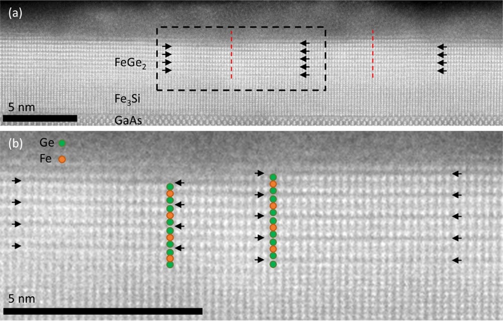
Although it was expected that pure germanium would form during this solid-phase epitaxy, the researchers observed something else entirely. A strong diffusion of iron into the germanium film was detected at relatively low crystallization temperatures. Moreover, instead of pure germanium with a diamond structure, an epitaxial film with iron content was obtained. High-angle annular dark-field (HAADF) scanning transmission electron microscopy (STEM) confirmed that the resulting crystal had a different metastable crystal structure to what was expected. The figure below shows the heterostructure produced after the annealing process.

STEM images taken of (a) the heterostructure produced after the annealing process, and (b) a magnified image of the dotted black box showing the vacant layers
Novelty in findings
Phase transformations are one of the most fascinating phenomena in nature. Observing such transformations in real time and with the resolution of individual atoms could revolutionize our understanding of their chemical and physical processes. This research demonstrates that a novel crystal phase of FeGe₂ can be interfaced from two materials with vastly different physical properties: Fe₃Si, a ferromagnet, interfaced with amorphous germanium, a semiconductor. Terker and his colleagues were able to demonstrate that a hybrid sample preparation approach can yield thin samples suitable for high resolution HAADF STEM while at the same time retaining the sample composition and structure. This approach could be applied to many different heterostructures and lead to a much broader applicability of the in situ TEM method in the study of phase transformations.

“For the atomic scale investigation of small nanostructures at high temperatures, the reduction of sample drift is of paramount importance. The new generation of DENSsolutions Wildfire Nanochips offer the ideal solution for this due to their small and reproducible bulging. Their robustness also enables an easy and safe transfer of the specimen lamella of any form or sample geometry.”
Markus Terker
PhD Student | Paul-Drude-Institut in Berlin, Germany
Original article:
Discover our Wildfire solution:
Discover more publications made possible by Wildfire:

Visualizing the structural evolution of thermally-decaying platinum nanowires
Using our Wildfire system, scientists gain an exceptional in-depth understanding of the morphological changes of platinum nanowires at certain temperatures

