DENSsolutions forms new and exclusive partnership with Funa Scientific in China

DENSsolutions forms new and exclusive partnership with Funa Scientific in China

We are excited to announce that DENSsolutions has joined forces with Funa Scientific, our new dedicated distributor in China.

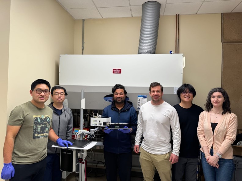
From left to right: Aaron Wan, Leo Li, Dan Zhou, Anton Qiu, Flora Cen, Simon Zhuang and Jerry Zhu

In the pursuit to strengthen and grow our business operations in China, DENSsolutions has partnered with Funa Scientific Co. – an established player in the electron microscopy industry. With this partnership, we plan to improve the speed and quality of our service and application support for our valued users in China. Moreover, we hope to make beneficial resources more accessible to local existing and potential customers, including user trainings, application support, webinars and publications. We are confident that this partnership will be fruitful for all parties involved, and most importantly for our customers. In this article, we introduce Funa Scientific so you can learn more about their services and values, as well as what to expect in the near future.

About Funa Scientific

Founded in 2012, Funa Scientific is a key provider of desktop scanning electron microscopes for universities, enterprises and research institutes. Importantly, they also help top overseas high-tech instrument manufacturers build a complete technical support and after-sales service system in the Chinese market, assisting users in scientific research innovation and problem-solving. At the very heart of the company is their customer-centric approach, whereby the innovation of products and the progress of the company are inseparable from the support of customers. Funa Scientific has an expansive customer base, including users from the most well-known enterprises and institutions around the world, accounting for 80% of the Fortune Global 500 companies, like Sony, Johnson Matthey, NASA and Siemens.

Funa Scientific conducts business in various regions of China, and each region has numerous sales engineers, application engineers and after-sales engineers. The company has testing centres and after-sales service centres in major cities across China, including Shanghai, Beijing, Guangzhou, and Chengdu.

Through long-term cooperation with key players in the microscopy industry to develop products such as the Thermo Fisher Scientific desktop scanning electron microscopes, VSParticle’s nano-research platform, Technoorg Linda’s Ar+ ion beam milling system and Forge Nano’s atomic layer deposition solutions, they have accumulated rich experience in the electron microscopy industry and nanoscale research technology. 

A bright future ahead

From this point onwards, Funa Scientific is the official distributor and business partner of DENssolutions in the Chinese market, fully responsible for the marketing, sales and service activities in China surrounding our solutions. Currently, Funa Scientific is working on setting up a dedicated local application research team and a Chinese website to be launched in the near future, which will feature the latest information about our advanced solutions and in situ microscopy news. Given Funa Scientific’s extensive expertise in the Chinese market, we are confident that this partnership will enable us to deliver our innovative solutions to a wider audience and better serve our customer base in China. We truly look forward to working closely with Funa Scientific to realize the bright future ahead.

Contact

If you have any questions for Funa Scientific, please reach out to their Product Director, Aaron Wan via email: aaron.wan@phenom-china.com or telephone: +8618516023887. Moreover, if you are based in China, we warmly encourage you to follow our WeChat account, run by Funa Scientific, so you can get all the latest updates. You can do so via this link or by scanning the following QR code. 

Subscribe to our newsletter to stay up-to-date with the latest in situ microscopy news.

DENSsolutions’ Lightning system helps uncover the interaction mechanism in reactive metal-ceramic system, Al-SiC

DENSsolutions’ Lightning system helps uncover the interaction mechanism in reactive metal-ceramic system, Al-SiC

Using the DENSsolutions Lightning system, researchers were able to provide an electrical, chemical and structural analysis of the Al–amorphous SiO₂–SiC interface at high temperatures.

Original article by Adabifiroozjaei et al.

The use of hybrid materials containing both metals and ceramics has become increasingly popular within manufacturing and microelectronic industries due to their optimized and well-balanced properties. Aluminum-silicon carbide (Al-SiC) is a widely known metal-ceramic composite material, commonly used in microelectronic packaging for automotive and aerospace applications. In Al-SiC an amorphous oxide layer (AOL) of SiO₂ is known to exist between the Al and SiC. Notably, the mechanism of interaction between the reactive metal (Al) and ceramic (SiC) and the AOL (SiO₂) under the heat-treatment process is still not well-understood. In fact, numerous theories about the interaction mechanism have been proposed over the past few decades. The major problem is that the studies conducted so far, regardless of the mechanism proposed in them, were ex situ and therefore not capable of resolving the atomic-scale nanostructural and chemical changes occurring at the interfaces during the heat-treatment process. In a recent paper published in the Journal of Materials Science, involving our valued users at TU Darmstadt, Dr. Esmaeil Adabifiroozjaei and Dr. Leopoldo Molina-Luna, the DENSsolutions Lightning system was utilized to reveal the evolution mechanism of the Al–AOL–SiC system under heating and biasing conditions. This study involved a team of researchers from institutes all over the world, including the University of Tabriz in Iran, NIMS and Shibaura Institute of Technology in Japan, and UNSW Sydney in Australia. 

Sample preparation

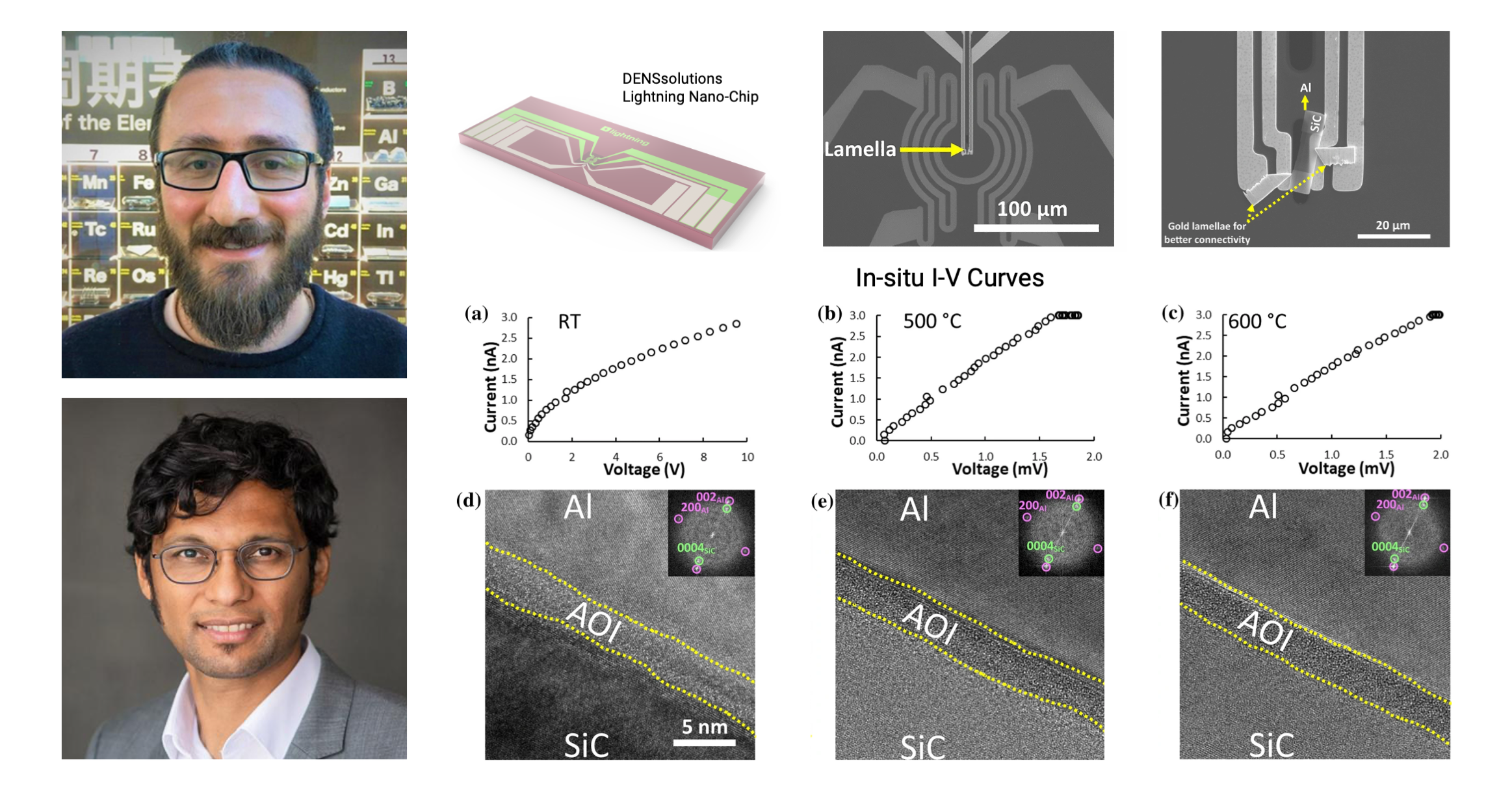
The first step for Dr. Adabifiroozjaei and his fellow collaborators was to carefully prepare the Al-SiC sample. After ultrasonically cleaning the SiC wafer, removing the oxide layer and allowing its regrowth by inserting the wafer into a desiccator, an Al layer with a thickness of ~1 µm was sputtered on the wafer using Shibaura’s CFS-4EP-LL sputtering machine. Next, in order to prepare the lamella, the researchers applied focused ion beam milling using JEOL’s JIB-4000 FIB. The prepared lamella was then loaded onto the DENSsolutions Lightning Nano-Chip (see Figure 1a). The low- and high-magnification scanning electron microscopy (SEM) images of the chip and the loaded lamella are shown below in Figure 1b) and 1c), respectively. Next, an Au lamella was prepared by FIB and connected to Al–AOL–SiC lamella and chip in order to ensure electrical current passes through Al–AOL–SiC lamella.

Figure 1: a) DENSsolutions Lightning Nano-Chip used for the in situ heating and biasing experiment, b) low- c) and high-magnification SEM images of the loaded lamella on the Nano-Chip, respectively.

Experimental results

The researchers performed EDX and EELS elemental mapping to determine the chemical composition of the phases across the Al–AOL–SiC interface. The EDS mapping of the interface is shown in Figure 2a), while the high-resolution EELS elemental mapping of the interface is shown in Figure 3b) – both of which reveal the consistent presence of a narrow oxide layer with a thickness in the range of 3–5 nm. 

Figure 2: a) EDS elemental mapping of Al–AOL–SiC interface, showing the presence of the AOL, b) STEM-HAADF image of Al–AOL–SiC interface and its EELS map profile.

Next, the researchers began with the in situ heating and biasing experiment to study the electrical characteristics of the lamella. First, a compliance current was set to 3 nA, then the voltage required to reach such a current was recorded at each temperature. The acquired I–V curves for room temperature, 500 ° and 600 °C after 30 minutes of application of the field are presented in Figure 3a–c), respectively. The I–V curves and high resolution TEM images (shown in Figure 3d–f) indicate that the resistivity of the Al–AOL–SiC device decreased three orders of magnitudes at 500 °C with no apparent change in the nanostructure. 

Figure 3: a), b), and c) show the I–V curves of Al–AOL–SiC interface measured at room temperature, 500° and 600 °C, respectively. d), e), and f) show the high-magnification images of Al–AOL–SiC interface from a small area of low-magnification images.

The chemical changes occurring at the interface during the heating process were investigated on another lamella using the same DENSsolutions Lightning holder, but on a Wildfire (heating-only) Nano-Chip. HAADF-STEM images and EELS chemical profiles were acquired and the results are shown in Figure 4 below. 

Figure 4: a), b), c ) and d) show changes in chemistry (line profiles of Al (Aqua), Si (Violet), C (Lime), and O (Yellow)) of Al–AOL–SiC interface at room temperature (25°), 550°, 500° and 600 °C, respectively.

During this analysis, the researchers observed that at 550 °C, the AOL width was reduced, which was specifically due to AOL dissolution into the Al. Moreover, the analysis of the structural changes at the interface nanostructure at 600 °C showed that the dissolution of the SiO₂ amorphous layer resulted in the formation of α-AlO and Si within the Al. In contrast, the elemental interdiffusion (Al³⁺ ⇄ Si⁴⁺) between Al and SiC was observed to occur, resulting in formation of AlC. From the results, we can infer that the reaction mechanism between Al and crystalline SiC is different with that between Al and SiO₂ amorphous phase.

Conclusion

Dr. Adabifiroozjaei and his fellow collaborators performed a comprehensive in situ STEM heating and biasing study using the DENSsolutions Lightning system, investigating the electrical, chemical and microstructural features of the interface of a Al–AOL–SiC system. Performing this study under an ultrahigh resolution of 4 Å allowed the researchers to confirm, for the first time in literature, that the reaction mechanism between reactive Al and crystalline SiC is different than between Al and amorphous SiO₂. Specifically, they found that whereas the reaction between SiO₂ and Al follows the dissolution mechanism, the reaction between SiC and Al proceeds through elemental interdiffusion. Importantly, these findings might be applicable to other reactive metal-ceramic systems that are currently used in manufacturing and electronic industries.

“With the stability and accuracy provided by DENSsolutions Lightning system, we could reveal features of an interfacial interaction in a common metal-ceramic system (Al-SiC) that were not previously observed. Such studies at very high resolution are absolutely necessary for the understanding and future development of composite materials at elevated temperatures.” 

Prof. Dr. Leopoldo Molina-Luna   Professor  |  TU Darmstadt

Original article:


Discover our Lightning solution:

Discover more publications made possible by Lightning:

Thomas article feature image

Liquid flow control: Unlock untapped research capabilities within in situ LPEM

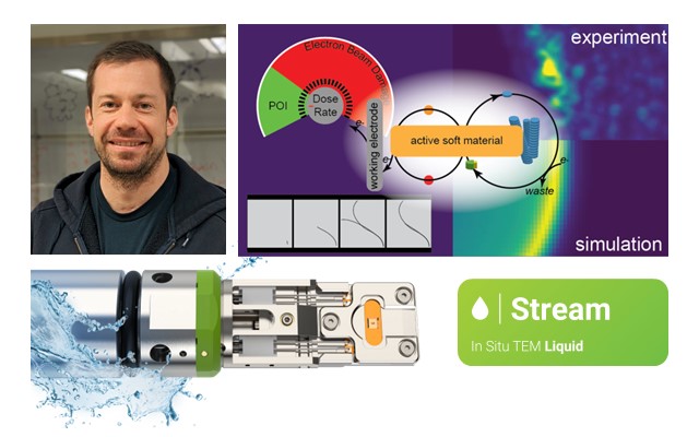
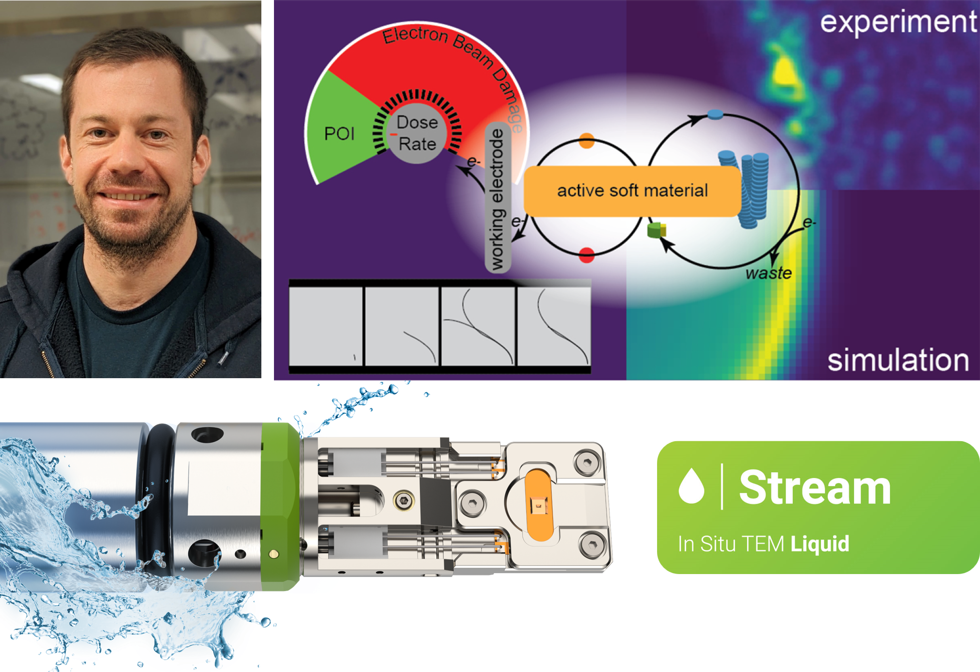
Using the DENSsolutions Stream system, researchers were able to create a highly controlled chemical environment for visualizing the nanoscale metallic electrodeposition of copper crystals.

Subscribe to our newsletter to stay up-to-date with the latest in situ microscopy news.

DENSsolutions successfully installs another Climate system in Japan, at JFCC

DENSsolutions successfully installs another Climate system in Japan, at JFCC

Top row – from left to right: Mr. Suzuki (Nano Tech Solutions), Mr. Anada (JFCC), Dr. Lars van der Wal (DENSsolutions) and Mr. Hirai (JEOL). Bottom row – from left to right: Mr. Fukunaga (JEOL), Mr. Jinbo (JEOL) and Mr. Hisada (JEOL).

We are proud to announce that DENSsolutions has installed another Climate system in Japan, at the Japan Fine Ceramics Center, located in Nagoya, a highly populated Japanese port city. In this article, we interview Dr. Satoshi Anada, Senior Researcher at the Nanostructures Research Lab in JFCC, to learn more about their microscopy facility, its research direction, as well as how our Climate system is advancing their research.

Can you tell me about Japan Fine Ceramics Center and its research and development initiatives?

Japan Fine Ceramics Center (JFCC) was established back in 1985, with the goal of improving the quality of fine ceramics mainly through integrated testing and evaluation systems. JFCC has numerous business activities, one of which is the research and development (R&D) of materials, manufacturing technology and evaluation technology. Our R&D initiatives are focused on obtaining technological solutions to problems related to the environment, energy and safety. We have two main laboratories: 1) the Materials R&D Lab and 2) the Nanostructures Research Lab. The Materials R&D Lab focuses on the development of highly functional and novel materials (mainly ceramics) by improved process control, whereas the Nanostructures Research Lab focuses on the development and enhancement of state-of-the-art electron microscopy and related technologies. At the Nanostructures Research Lab, we have a high-end electron microscope – the JEOL JEM-ARM300F2 Grand ARM. This microscope enables us to observe samples at ultra-high spatial resolution with highly sensitive analysis over a wide range of accelerating voltages.”

What type of applications are the users at the Nanostructures Research Lab interested in using the Climate G+ system for?

“Users at the Nanostructures Research Lab are interested in applying the DENSsolutions Climate system to record operando TEM observations of battery and catalyst materials. We aim to understand where and how reactions take place, and which conditions enhance the performance of those materials. Moreover, we are interested in the electrochemical oxidation of materials in reaction with oxidants such as oxygen and hydrogen.”

What particular features of the DENSsolutions Climate G+ system attracted you to the system? 

“In order to understand factors and mechanisms related to the performance of battery and catalyst materials, it is important to observe their reactions in the actual environments in which they are used. The Climate system has the ability to flexibly and rapidly adjust gas composition, temperature, flow and pressure, which enables us to observe our battery and catalyst materials under various experimental conditions. This is capability is particularly what attracted us to the solution.”

In your experience so far, how have you found working with the Climate G+ system?

“The preliminary processes including the assembly of the Climate Nano-Reactor and leak testing are quite straightforward, assisted by the well-established Climate manual and software. With the Climate system, we have been able to perform numerous experiments without running into any leakage issues. Moreover, we are particularly impressed with the stability of the system even at extremely high temperatures.”

Dr. Satoshi Anada
Senior Researcher | Japan Fine Ceramics Center

Dr. Satoshi Anada received his Ph.D. degree in Engineering, Material Science, from Osaka University. Previously, he was working as a Specially Appointed Assistant Professor in the Research Center for Ultra-High Voltage Electron Microscopy at Osaka University. Currently, Dr. Anada is working as a Senior Researcher in the Japan Fine Ceramics Center (JFCC). His research was focused on the electromagnetic analysis of functional materials and devices using transmission electron microscopy, and now particularly on different microscopic measurement informatics.

Discover Dr. Anada’s publications:


Learn more about Climate:


Discover publications made possible by Climate:

Subscribe to our newsletter to stay up-to-date with the latest in situ microscopy news.

Meet Dr. Evgeniya Pechnikova, our new Senior Applications Development Scientist

Meet Dr. Evgeniya Pechnikova, our new Senior Applications Development Scientist

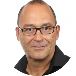
We are happy to announce that DENSsolutions has expanded the team with a wonderful new colleague – Dr. Evgeniya Pechnikova.

In the pursuit to grow our applications development for the DENSsolutions Stream system and other future product lines, we recently welcomed Dr. Evgeniya Pechnikova to the team – our new Senior Applications Development Scientist. Evgeniya has years of experience and high-level technical expertise in electron microscopy (EM), including cryogenic-EM, tomography and data processing techniques. Her role at DENSsolutions will be focused on developing novel in situ liquid EM applications that demonstrate the power of our solutions. She will also be working on creating new techniques and methodologies that will support the research of our customers, as well as perfecting our demonstration and installation protocols. We are thrilled to have Evgeniya join the DENSsolutions family and look forward to the valuable contributions she will make to the team on both a personal and professional level. In this article, we have asked Evgeniya to introduce herself so you can learn more about her extensive experience and her new role at DENSsolutions.

Meet Dr. Evgeniya Pechnikova

“My name is Evgeniya Pechnikova, and I was born and raised in Moscow, Russia. I have a lot of love for adventure and history, and enjoy travelling around the world to explore ruins of ancient civilizations. I’m also an avid fan of photography, Latin social dances like salsa and tango, as well as playing badminton and a game known as ‘werewolves’!

I have always been drawn to different spheres of science. That is why for my higher education, I decided to enrol in Lomonosov Moscow State University‘s biological faculty. As they had a very broad program there, I had the opportunity to learn about a wide range of subjects, starting with mathematics and physics and ending up with biochemistry, plant physiology and even drawing.

During my master’s degree, I was introduced to the world of electron microscopy and was completely fascinated by its combination of science and photography – two topics that have always been a passion of mine. To add another dimension to my work, I found a PhD position in the field of cryo-EM and 3D reconstruction, working on investigating the structure and function of capsids of a helical plant virus. My PhD project was a result of a collaboration between Lomonosov Moscow State University, Institute of Crystallography in Moscow and Birkbeck, University of London. During this PhD, I worked in close collaboration with structural biologists that were highly experienced in cryo-EM and image processing before the new detector technology popularised the technique to a broader base of scientists. This was an incredibly enriching experience and certainly shaped my career path moving forward.

After completing my PhD, I joined Thermo Fisher Scientific in the Netherlands where I worked as an Applications Scientist in the Eindhoven NanoPort facility – a state-of-the-art electron microscopy facility that provides users with hands-on experience with numerous analytical techniques. During this role, I was responsible for providing training and demonstrations for life science TEM equipment. I was also in frequent collaboration with the R&D department to translate customer needs into applications development, and to test new hardware and software tools. As a result of this work, I was able to play a role in accelerating the new-resolution revolution that has bloomed in cryo-EM over the past couple years. Importantly, this role made me realize that trying new tools to solve long-standing problems is what excites me most. 

Now, as a Senior Applications Development Scientist at DENSsolutions, I have the unique opportunity to combine and explore two cutting-edge technologies, MEMS and cryo-EM. My top priority is to boost applications development and create working protocols that showcase the advantages of DENSsolutions’ MEMS technology within in situ liquid EM. I look forward to being actively involved in hands-on support during on-site and remote product demonstrations, as well as working with other departments to translate customer needs into workable solutions. I am excited to take on this new challenge and am confident that I will be able to make a meaningful contribution to the company, our customers and science as a whole.”

Get in touch with Evgeniya via:

Subscribe to our newsletter to stay up-to-date with the latest in situ microscopy news.

Meet our new Vice President of Sales and Business Development, Hans Radhoe

Meet our new Vice President of Sales and Business Development, Hans Radhoe

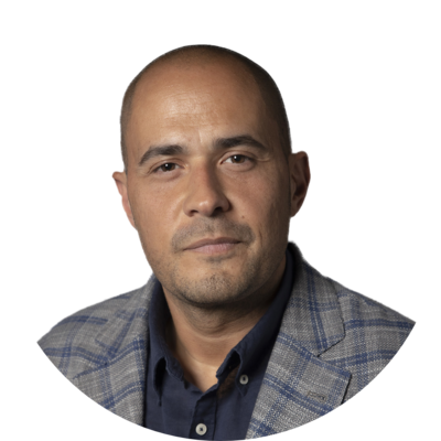
We are excited to announce the expansion of our team with our new colleague, Hans Radhoe.

Despite being a small company in the canal-ringed city of Delft, DENSsolutions has always been highly ambitious, with its sights set on disruptive growth and innovation. Keeping in line with this, we wanted to expand our team with someone who could lead our business development, with a focus on the discovery of new growth opportunities for the company and making our many visions a reality. We are happy to have found just the right person for this position – Hans Radhoe, our new Vice President of Sales and Business Development. With over 25 years of experience in business and development within fields such as life science and materials science, Hans has an extensive understanding of lead generation, advancing business strategy and the sales cycle process within diverse scientific markets. His role at DENSsolutions will focus on finding avenues of growth for the company and leading numerous aspects of the sales process, from prospecting and go-to-market strategies to customer relationship management. In this article, we have asked Hans to introduce himself so you can learn more about his education, experience and role at DENSsolutions. 

Meet Hans Radhoe

“My name is Hans Radhoe, and I was born in Suriname, a country in South America in the Amazon. At just 17 years old, I left Suriname with the bright intention to study medicine in the Netherlands. I had no knowledge at that time, however, that there was a lottery system in place in the Netherlands for being admitted into any of the medical schools in the country. As it turned out, I was not one of those selected to move forward in the admission process, which forced me to think of an alternative study to pursue.

This chain of events catapulted the start of my education in the field of biotechnology, which I studied at the Polytechnical Faculty in Delft. Studying biotechnology felt like an excellent choice for me since it not only piqued my interest, but was also a hot topic in the 80s and beyond. After finishing my Bachelor studies, my fascination with the environment led me to pursue a Master’s degree in Environmental Management at Open University in Heerlen, a small city in the southeast of the Netherlands bordering Germany.

After graduating, I took on a position for a couple years with the task of setting up a mycoplasma and virology lab in accordance with CGMP guidelines. In this role, I managed to upscale Mycoplasma testing services for the pharmaceutical industry. I then worked at Centocor in Leiden for a short while, which is a biotech subsidiary of Johnson & Johnson. During this role, I was responsible for the production of biologic drugs involving monoclonal antibody technology, such as Remicade – a drug used to treat a number of autoimmune diseases like rheumatoid arthritis. It was particularly during this role that I gained hands-on experience in cell and gene therapy. 

Shortly after, I made the switch from lab to business because I became more and more passionate about perceiving and fulfilling the commercial needs of others. During my business jobs, I realized how imperative it is to be able to listen intently and actively when in communication with customers. This encouraged me to take a Master’s in Counselling and Coaching, which is part of the Psychology study at the Radboud University Nijmegen. Although the intention of pursuing this Master’s was to use the knowledge learnt to enhance my communication with clients, I found myself applying it in the volunteer work that I did next to my job at the time. This volunteer work involved coaching cancer patients at the Nederlandse Federatie van Kankerpatiëntenorganisaties, which I happened to stumble upon when seeing an advertisement from the organisation on TV. 

Further down the line in my career, after many enriching vocational experiences, I started working as the Sales Director at Amsterdam Scientific Instruments (ASI) – a spin-off company from Nikhef, which is a Dutch research institute for particle physics. ASI specializes in the design and manufacturing of advanced detector solutions for all kinds of particles, such as electrons. Indeed, it was particularly during this position that I stepped into the world of electron microscopy, which I found to be rather fascinating.

This then brings me to today, where I now have the role of Vice President of Sales and Business Development at DENSsolutions, a company that develops advanced electron microscopy solutions. I have actually been following DENSsolutions for a long time since a friend of mine worked here, and I have witnessed for myself the rapid innovation of the company in the past few years. Generally, in the span of my career, I have been active in numerous scientific markets all over the world and in many different positions, including account management, sales and business development. In my new role, I will be in charge of increasing the company’s presence in existing markets, as well as forming strategic partnerships that open up entirely new ones. I look forward to applying my extensive knowledge gained over the past two decades into this new role, and being part of a fantastic team so focused on continuous cooperation and innovation.”

Get in touch with Hans via:

Subscribe to our newsletter to stay up-to-date with the latest in situ microscopy news.