DENSsolutions’ Lightning system helps uncover the interaction mechanism in reactive metal-ceramic system, Al-SiC

DENSsolutions’ Lightning system helps uncover the interaction mechanism in reactive metal-ceramic system, Al-SiC

Using the DENSsolutions Lightning system, researchers were able to provide an electrical, chemical and structural analysis of the Al–amorphous SiO₂–SiC interface at high temperatures.

Original article by Adabifiroozjaei et al.

The use of hybrid materials containing both metals and ceramics has become increasingly popular within manufacturing and microelectronic industries due to their optimized and well-balanced properties. Aluminum-silicon carbide (Al-SiC) is a widely known metal-ceramic composite material, commonly used in microelectronic packaging for automotive and aerospace applications. In Al-SiC an amorphous oxide layer (AOL) of SiO₂ is known to exist between the Al and SiC. Notably, the mechanism of interaction between the reactive metal (Al) and ceramic (SiC) and the AOL (SiO₂) under the heat-treatment process is still not well-understood. In fact, numerous theories about the interaction mechanism have been proposed over the past few decades. The major problem is that the studies conducted so far, regardless of the mechanism proposed in them, were ex situ and therefore not capable of resolving the atomic-scale nanostructural and chemical changes occurring at the interfaces during the heat-treatment process. In a recent paper published in the Journal of Materials Science, involving our valued users at TU Darmstadt, Dr. Esmaeil Adabifiroozjaei and Dr. Leopoldo Molina-Luna, the DENSsolutions Lightning system was utilized to reveal the evolution mechanism of the Al–AOL–SiC system under heating and biasing conditions. This study involved a team of researchers from institutes all over the world, including the University of Tabriz in Iran, NIMS and Shibaura Institute of Technology in Japan, and UNSW Sydney in Australia. 

Sample preparation

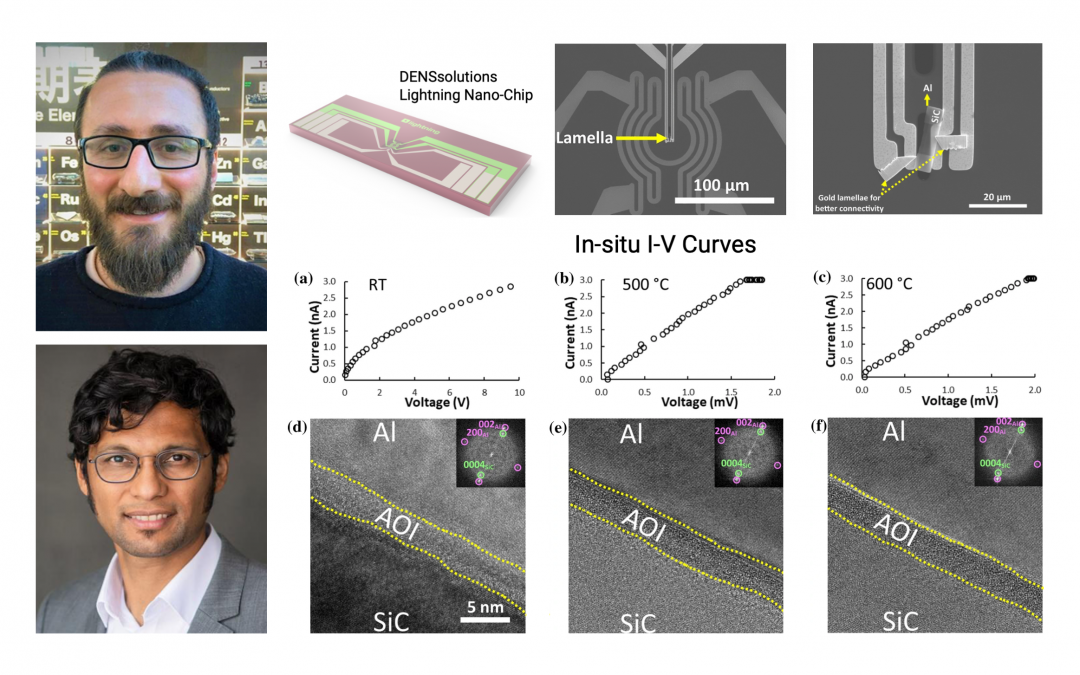
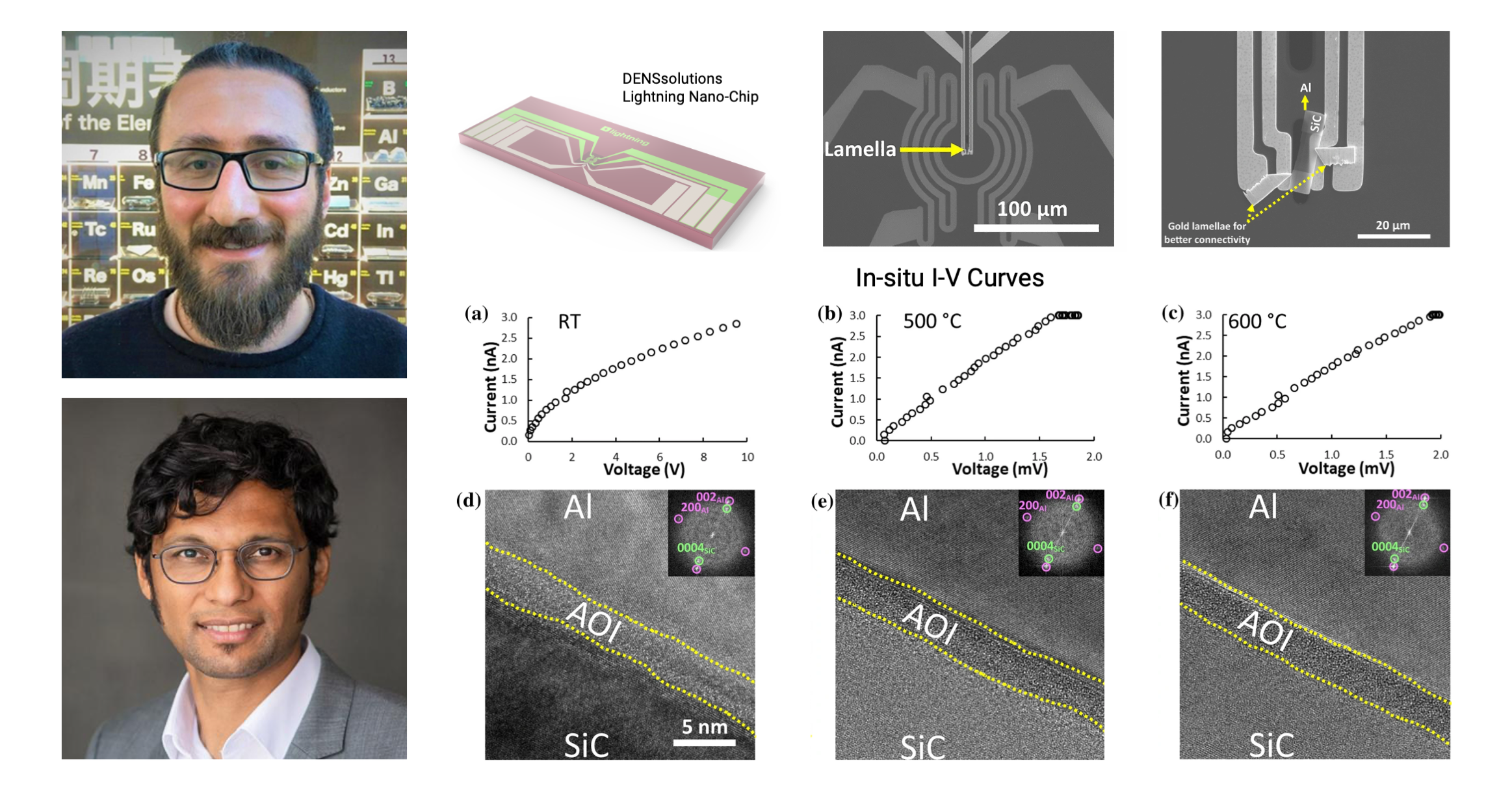
The first step for Dr. Adabifiroozjaei and his fellow collaborators was to carefully prepare the Al-SiC sample. After ultrasonically cleaning the SiC wafer, removing the oxide layer and allowing its regrowth by inserting the wafer into a desiccator, an Al layer with a thickness of ~1 µm was sputtered on the wafer using Shibaura’s CFS-4EP-LL sputtering machine. Next, in order to prepare the lamella, the researchers applied focused ion beam milling using JEOL’s JIB-4000 FIB. The prepared lamella was then loaded onto the DENSsolutions Lightning Nano-Chip (see Figure 1a). The low- and high-magnification scanning electron microscopy (SEM) images of the chip and the loaded lamella are shown below in Figure 1b) and 1c), respectively. Next, an Au lamella was prepared by FIB and connected to Al–AOL–SiC lamella and chip in order to ensure electrical current passes through Al–AOL–SiC lamella.

Figure 1: a) DENSsolutions Lightning Nano-Chip used for the in situ heating and biasing experiment, b) low- c) and high-magnification SEM images of the loaded lamella on the Nano-Chip, respectively.

Experimental results

The researchers performed EDX and EELS elemental mapping to determine the chemical composition of the phases across the Al–AOL–SiC interface. The EDS mapping of the interface is shown in Figure 2a), while the high-resolution EELS elemental mapping of the interface is shown in Figure 3b) – both of which reveal the consistent presence of a narrow oxide layer with a thickness in the range of 3–5 nm. 

Figure 2: a) EDS elemental mapping of Al–AOL–SiC interface, showing the presence of the AOL, b) STEM-HAADF image of Al–AOL–SiC interface and its EELS map profile.

Next, the researchers began with the in situ heating and biasing experiment to study the electrical characteristics of the lamella. First, a compliance current was set to 3 nA, then the voltage required to reach such a current was recorded at each temperature. The acquired I–V curves for room temperature, 500 ° and 600 °C after 30 minutes of application of the field are presented in Figure 3a–c), respectively. The I–V curves and high resolution TEM images (shown in Figure 3d–f) indicate that the resistivity of the Al–AOL–SiC device decreased three orders of magnitudes at 500 °C with no apparent change in the nanostructure. 

Figure 3: a), b), and c) show the I–V curves of Al–AOL–SiC interface measured at room temperature, 500° and 600 °C, respectively. d), e), and f) show the high-magnification images of Al–AOL–SiC interface from a small area of low-magnification images.

The chemical changes occurring at the interface during the heating process were investigated on another lamella using the same DENSsolutions Lightning holder, but on a Wildfire (heating-only) Nano-Chip. HAADF-STEM images and EELS chemical profiles were acquired and the results are shown in Figure 4 below. 

Figure 4: a), b), c ) and d) show changes in chemistry (line profiles of Al (Aqua), Si (Violet), C (Lime), and O (Yellow)) of Al–AOL–SiC interface at room temperature (25°), 550°, 500° and 600 °C, respectively.

During this analysis, the researchers observed that at 550 °C, the AOL width was reduced, which was specifically due to AOL dissolution into the Al. Moreover, the analysis of the structural changes at the interface nanostructure at 600 °C showed that the dissolution of the SiO₂ amorphous layer resulted in the formation of α-AlO and Si within the Al. In contrast, the elemental interdiffusion (Al³⁺ ⇄ Si⁴⁺) between Al and SiC was observed to occur, resulting in formation of AlC. From the results, we can infer that the reaction mechanism between Al and crystalline SiC is different with that between Al and SiO₂ amorphous phase.

Conclusion

Dr. Adabifiroozjaei and his fellow collaborators performed a comprehensive in situ STEM heating and biasing study using the DENSsolutions Lightning system, investigating the electrical, chemical and microstructural features of the interface of a Al–AOL–SiC system. Performing this study under an ultrahigh resolution of 4 Å allowed the researchers to confirm, for the first time in literature, that the reaction mechanism between reactive Al and crystalline SiC is different than between Al and amorphous SiO₂. Specifically, they found that whereas the reaction between SiO₂ and Al follows the dissolution mechanism, the reaction between SiC and Al proceeds through elemental interdiffusion. Importantly, these findings might be applicable to other reactive metal-ceramic systems that are currently used in manufacturing and electronic industries.

“With the stability and accuracy provided by DENSsolutions Lightning system, we could reveal features of an interfacial interaction in a common metal-ceramic system (Al-SiC) that were not previously observed. Such studies at very high resolution are absolutely necessary for the understanding and future development of composite materials at elevated temperatures.” 

Prof. Dr. Leopoldo Molina-Luna   Professor  |  TU Darmstadt

Original article:


Discover our Lightning solution:

Discover more publications made possible by Lightning:

Thomas article feature image

Liquid flow control: Unlock untapped research capabilities within in situ LPEM

Using the DENSsolutions Stream system, researchers were able to create a highly controlled chemical environment for visualizing the nanoscale metallic electrodeposition of copper crystals.

Subscribe to our newsletter to stay up-to-date with the latest in situ microscopy news.

Improved FIB lamella preparation

Improved FIB lamella preparation

A conversation with our Product Manager Dr. Yevheniy (Gin) Pivak on the new FIB stub 3.0

DENSsolutions introduces the 3rd generation of the FIB stub which enables researchers to prepare a lamella and place it directly on the Nano-Chip, all inside the FIB. In this version, many improvements were made to make the FIB sample preparation easier, safer and quicker. The development of this new stub was headed by our Product Manager Dr. Yevheniy (Gin) Pivak in close collaboration with key partners like AEM, TU Darmstadt and EMAT, Antwerp.

Why was this new FIB stub designed?

Any TEM experiment starts with a good sample either it’s a nanoparticle, a FIB lamella, 2D material or a nanowire. The FIB sample is the most complicated among others, especially when it comes to preparing lamellas onto MEMS-based Nano-Chips.
Several years back, when the users’ knowledge on FIB lamella preparation onto MEMS-based Nano-Chips was still very limited and the field itself was premature, DENSsolutions developed the first version of a FIB stub which had two inclined sides of 45 degrees on which the sample and Nano-Chip could be positioned. This stub simplified the sample preparation process by allowing the user to prepare and transfer a lamella onto the Nano-Chip in one go without breaking the vacuum of the FIB chamber, thus saving operation time. Since then version 2.0 was released, which kept the main design features like the two inclined sides but improved the sample and Nano-Chip positioning and clamping.
In the meantime, hundreds of lamellas were successfully prepared and placed onto Nano-Chips but many users still encounter challenges during the process. First of all, the issues come from an uncommon geometry that the users need to work with; the lamella preparation and the lift out need to be done at 45 and 55 stage tilt angles. On top of that, the users suffer from poor imaging, especially at low accelerating voltage and a charging effect. The positioning of the Nano-Chip and the clamping mechanism, that is also there for grounding purposes is not optimal, making the operation not very user-friendly. Because the height of the sample and the Nano-Chip on the FIB stub can differ quite a bit, there also is a safety concern.
In recent years more and more people are interested in in-situ TEM Biasing and Biasing & Heating experiments. The majority of those samples are FIB lamellas and the requirements towards the samples for electrical measurements are much stricter compared to heating experiments with various pitfalls along the way. A new approach aiming to avoid short circuiting and reiteration of biasing and biasing & heating lamellas is required.

What are the benefits of this new FIB stub?

The new FIB stub solves a number of limitations of the previous versions.

At first, the new 3.0 stub incorporates an additional flat side for placing the samples that ensures a conventional geometry and the very same and the well-known process used by any FIB operator when making and lifting out the lamella.

The revised geometry improves the quality of imaging even during the low kV milling and polishing steps. Additionally, the charging effect is reduced due to a more effective grounding of the Nano-Chips’ contact pads.

A dedicated pocket and a smart clamping mechanism is introduced which drastically simplifies and speeds up the Nano-Chip loading and unloading, making it very user-friendly. It reduces the risk of breaking the membrane when handling the Nano-Chips and there is also no need to use sticky tapes to fix or to ground the Nano-Chip, which in turn makes the process a lot cleaner.

The design of the FIB stub brings the position of the sample and the Nano-Chip to a similar eucentric height, minimizing the possibility of crashing into the pole piece, the Gas Injection System or the manipulator during the operation.

What is the compatibility of the new FIB stub?

The new FIB stub is compatible with Thermo Fisher/FEI and JEOL dual beams. It’s suitable for various models like Strata DB235 (Thermo Fisher/FEI), Helios NanoLab 600 / 650 / G4 CX (Thermo Fisher/FEI), JIB 4600F (JEOL) and many more.
It’s also suitable for any Thermo Fisher (FEI) and JEOL double tilt Heating and/or Biasing Nano-Chips.

Who are the people that will benefit from it?

Any existing customers who own a double tilt Wildfire TF(FEI)/JEOL (Wildfire D6, Wildfire H+ DT), a Lightning HB TF(FEI)/JEOL (Lightning D6+) or a Lightning HB+ TF(FEI)/JEOL (Lighting D7+, Lightning D9+) system and works with FIB lamellas will definitely benefit from the new FIB stub.
New customers of Wildfire and Lightning systems planning to work with in situ heating samples or electronic devices like non-volatile memory based on resistive switching or phase change materials, solid state batteries, solar cells, etc will enjoy the sample preparation using the 3.0 stub

What kind of challenges were tackled during development?

As in many developments, the main goal is to create a really good product that can be used by most of the users. However, because there are many dual beams from different manufacturers out there with their own stage and column design, various manipulators, workflows, details, etc. that also can vary from site to site it is quite challenging to make one generic product that is suitable for everybody. It’s not possible to fulfil everyone’s needs, but we spent a lot of time trying to get the new FIB stub as versatile as possible.
In any case, product development is a dynamic process. As long as researchers find bottlenecks in their pursuit to get the right research results, we will focus our efforts to provide them with the right solution.

Did we cooperate with customers on this development?

Any product is meant to solve customers issues and limitations or create new opportunities. We make products for our customers and not for ourselves and there is no way to make a good product without customers involvement.
Following our strategy, we involved a number of our close collaborators during the development and testing of the new FIB stub project, namely EMAT (University of Antwerp) and AEM (University of Darmstadt). Additionally, more customers from Germany, UK, Singapore, Spain, Sweden, etc. were involved in the initial discussion phase to identify the current issues and limitations with the FIB lamella preparation.

Which future developments lie ahead?

In the near future, the intention is to verify the compatibility of the FIB stub 3.0 in Zeiss, Tescan and Hitachi dual beams.
If you are a proud owner of one of above-mentioned FIBs and you would be interested to test the new stub, please contact us.
On a longer term, we are working to further improve the electrical quality of lamellas and devices prepared on biasing and heating and biasing Nano-Chips. This next development is planned to be present at the EMC 2020 conference in Copenhagen. So, stay tuned!

5 reasons to get the new FIB stub:

Receive a quotation:

Do you want to receive great articles like this in your mailbox? Subscribe to our newsletter.

215