Behind the scenes of our MEMS production at EKL
See how we produce consistent high quality MEMS devices for our customers.
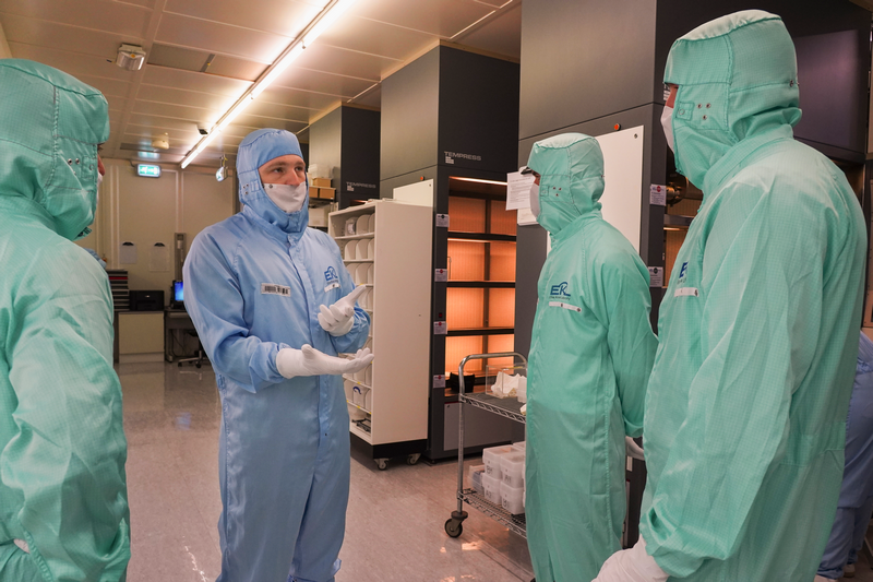
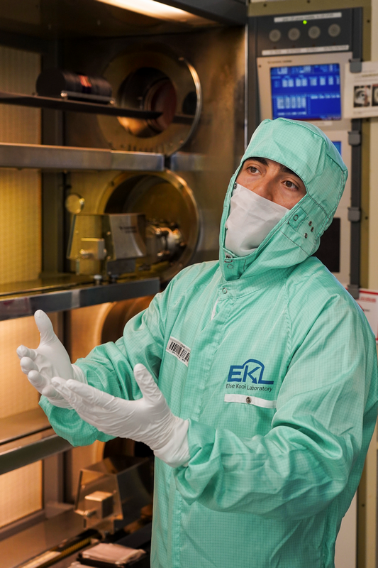
Process Engineer from EKL explaining the latest improvements to DENSsolutions quality control employees.
DENSsolutions and EKL (Else Kooi Laboratory) have been working together since the founding of our company in 2012. All our MEMS devices, from Wildfire chips to more intricate Stream Nano-Cells are developed in conjunction with this laboratory and produced here in Delft, the Netherlands. Being partly an academic laboratory, EKL is the perfect partner for us to develop innovative new ways to expose your sample to a variety of stimuli.

Bottom chips of our Stream Nano-Cell MEMS devices.
Rocket science
Chip production might not be as explosive as rocket science, but it is just as challenging. We produce numerous chips, and every single one is of consistent high quality which is especially challenging when you’re working on the sub micrometer scale. To ensure top production over so many chips, we need sophisticated processes. Luckily for us, we can count on a dedicated and enthusiastic team of experts at EKL that always strive to meet our demands.
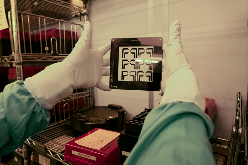
EKL employee showing the photomask for one of the layers required for the manufacturing of the Wildfire chips.
Overcoming challenges
So what does it actually take to produce these nanodevices? Since they are at the heart of our solutions, we take a lot of care in their manufacture.
We endeavour to make our MEMS devices precise and with tight tolerances, free of contamination, reproducible and affordable. It is precisely these values that drive our production process. Each step is carefully inspected for cleanliness, consistency and quality.
What is a MEMS device?
MEMS stands for Micro-Electro-Mechanical Systems. All our ‘sample carriers’ are MEMS devices. We normally don’t use the description ‘sample carriers’ because they do way more than just carrying the sample. They expose the specimen to a wide variety of stimuli and provide quantitative measurements. We talk about “Nano-Chips” for Wildfire and Lightning, but when we stack chips to form closed channels for gas or liquid we refer to them as “Nano-Reactors”, for Climate, and “Nano-Cells”, for Stream and Ocean.
Historically, the earliest microfabrication processes were used for integrated circuit production, but in the last decades extended and re-adapted microfabrication methods have led to new processes for MEMS development.
A small piece of dust on a smartphone chip is usually unnoticeable. However, even the smallest amount of dust on our MEMS device can obstruct the nanoscale view of a sample. Our MEMS must be extremely clean and this is inspected between the many stages of its production. Overall, the development of these types of devices brings challenges in many areas of science and engineering: chemistry, physics, materials science, fabrication processes, but it is also giving rise to many kinds of interdisciplinary research.
Ellipsometry is an optical technique used to investigate the dielectric properties of thin films.
Photolithography step to expose the photomask within the wafer.
Nanometer precision
Next to cleanliness we also place high demands on our chips in terms of specific features that are required to do research with a high level of reliability. Our Stream Nano-Cells, for instance, need to be able to guarantee the right liquid thickness irrespective of the tolerances of the o-ring that seals them. Similarly, the windows need to ensure a reliable control of the bulging and a constant viewing area. We use different etching and deposition steps to create the spacers inside your Nano-Cell that are responsible for channeling the liquid. Similarly, during the window formation, we have to etch away exactly the right amount of material underneath, while keeping the layer intact with a precision of nanometers.
For some mainstream applications, over-etching of a few nanometers might not be important. In our case, keeping a specific thickness out of spec might result in the need to throw away the whole wafer and start all over again. If we have already accomplished 70-80% of the process, you can imagine how precious this can be. So we have to constantly push the machines to their limits to make sure we just etch exactly the right amount, over and over again.
Did you know?
There are up to 25-30 machines involved in the production of our MEMS devices. Each of these machines has a set of unique variables that need to be just right. Think of pressure, power, chemistry of gases, temperature, frequency and time as some of the variables that have to be adjusted for the different machines in order to create the right recipe. Only by setting these in the right way, would the operator get the necessary chemical affinity and deposition/etching rates to successfully manufacture the chip that heats up your sample with super low drift.
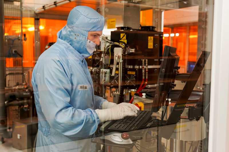
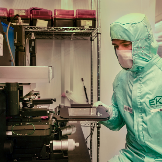
Process Engineer at EKL while adjusting the process recipe for one of the most crucial steps within the microfabrication.
Our MEMS are used in research as consumables. You might need to do many experiments using multiple chips to get the result that you want. So our MEMS have to be affordable to fit research budgets.
Each step of our workflow has been enhanced over the years to be as efficient as possible. This decreases lab time and cost, and ensures that each chip in a series has exactly the same specs. Your accuracy is our priority.
“We’re convinced that the MEMS devices are the core competence of our company. It is highly possible that high-impact advances will occur at the intersection of new process technologies and new architectures. Therefore, it’ll be our continuous job to push the limits in a well-planned, structured and innovative way”
Chief Technology Officer Dr. Hugo Perez Garza – DENSsolutions
See how we produce consistent high quality MEMS devices for our customers.
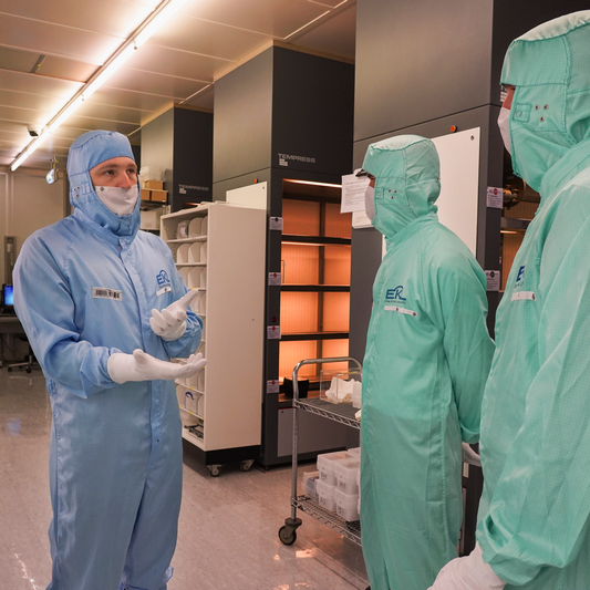
Process Engineer from EKL explaining the latest improvements to DENSsolutions quality control employees.
DENSsolutions and EKL (Else Kooi Laboratory) have been working together since the founding of our company in 2012. All our MEMS devices, from Wildfire chips to more intricate Stream Nano-Cells are developed in conjunction with this laboratory and produced here in Delft, the Netherlands. Being partly an academic laboratory, EKL is the perfect partner for us to develop innovative new ways to expose your sample to a variety of stimuli.
Bottom chips of our Stream Nano-Cell MEMS devices.
Rocket science
Chip production might not be as explosive as rocket science, but it is just as challenging. We produce numerous chips, and every single one is of consistent high quality which is especially challenging when you’re working on the sub micrometer scale. To ensure top production over so many chips, we need sophisticated processes. Luckily for us, we can count on a dedicated and enthusiastic team of experts at EKL that always strive to meet our demands.
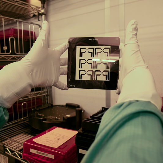
EKL employee showing the photomask for one of the layers required for the manufacturing of the Wildfire chips.
Overcoming challenges
So what does it actually take to produce these nanodevices? Since they are at the heart of our solutions, we take a lot of care in their manufacture.
We endeavour to make our MEMS devices precise and with tight tolerances, free of contamination, reproducible and affordable. It is precisely these values that drive our production process. Each step is carefully inspected for cleanliness, consistency and quality.
What is a MEMS device?
MEMS stands for Micro-Electro-Mechanical Systems. All our ‘sample carriers’ are MEMS devices. We normally don’t use the description ‘sample carriers’ because they do way more than just carrying the sample. They expose the specimen to a wide variety of stimuli and provide quantitative measurements. We talk about “Nano-Chips” for Wildfire and Lightning, but when we stack chips to form closed channels for gas or liquid we refer to them as “Nano-Reactors”, for Climate, and “Nano-Cells”, for Stream and Ocean.
Historically, the earliest microfabrication processes were used for integrated circuit production, but in the last decades extended and re-adapted microfabrication methods have led to new processes for MEMS development.
A small piece of dust on a smartphone chip is usually unnoticeable. However, even the smallest amount of dust on our MEMS device can obstruct the nanoscale view of a sample. Our MEMS must be extremely clean and this is inspected between the many stages of its production. Overall, the development of these types of devices brings challenges in many areas of science and engineering: chemistry, physics, materials science, fabrication processes, but it is also giving rise to many kinds of interdisciplinary research.
Ellipsometry is an optical technique used to investigate the dielectric properties of thin films.
Photolithography step to expose the photomask within the wafer.
Nanometer precision
Next to cleanliness we also place high demands on our chips in terms of specific features that are required to do research with a high level of reliability. Our Stream Nano-Cells, for instance, need to be able to guarantee the right liquid thickness irrespective of the tolerances of the o-ring that seals them. Similarly, the windows need to ensure a reliable control of the bulging and a constant viewing area. We use different etching and deposition steps to create the spacers inside your Nano-Cell that are responsible for channeling the liquid. Similarly, during the window formation, we have to etch away exactly the right amount of material underneath, while keeping the layer intact with a precision of nanometers.
For some mainstream applications, over-etching of a few nanometers might not be important. In our case, keeping a specific thickness out of spec might result in the need to throw away the whole wafer and start all over again. If we have already accomplished 70-80% of the process, you can imagine how precious this can be. So we have to constantly push the machines to their limits to make sure we just etch exactly the right amount, over and over again.
Did you know?
There are up to 25-30 machines involved in the production of our MEMS devices. Each of these machines has a set of unique variables that need to be just right. Think of pressure, power, chemistry of gases, temperature, frequency and time as some of the variables that have to be adjusted for the different machines in order to create the right recipe. Only by setting these in the right way, would the operator get the necessary chemical affinity and deposition/etching rates to successfully manufacture the chip that heats up your sample with super low drift.
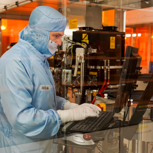
Process Engineer at EKL while adjusting the process recipe for one of the most crucial steps within the microfabrication.
Our MEMS are used in research as consumables. You might need to do many experiments using multiple chips to get the result that you want. So our MEMS have to be affordable to fit research budgets.
Each step of our workflow has been enhanced over the years to be as efficient as possible. This decreases lab time and cost, and ensures that each chip in a series has exactly the same specs. Your accuracy is our priority.
“We’re convinced that the MEMS devices are the core competence of our company. It is highly possible that high-impact advances will occur at the intersection of new process technologies and new architectures. Therefore, it’ll be our continuous job to push the limits in a well-planned, structured and innovative way”
Chief Technology Officer Dr. Hugo Perez Garza – DENSsolutions