Stream LPEM system wins the Microscopy Today 2020 Innovation award

Stream LPEM system wins the Microscopy Today 2020 Innovation award

A conversation with our CTO Dr. Hugo Pérez-Garza who has been leading the development of the award winning system.

DENSsolutions is one of this year’s winners of the Microscopy Today Innovation Award. At the 2020 Microscopy & Microanalysis Virtual Meeting, DENSsolutions Stream LPEM system has been recognized as one of the ten most innovative products of the year.

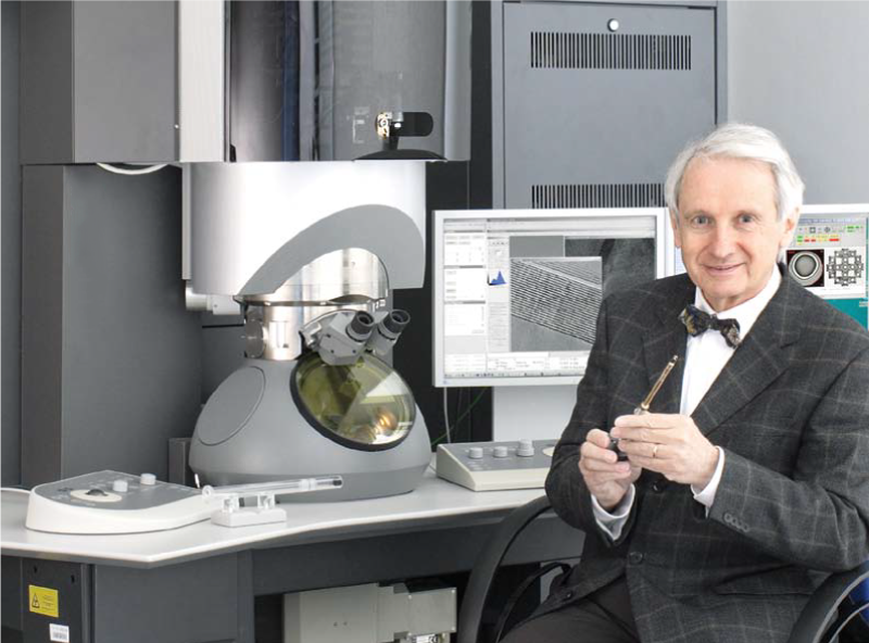
We interviewed CTO Dr. Hugo Pérez- Garza to learn exactly how the Stream system convinced the jury of its high degree of innovation that makes new scientific investigations possible. Below you will find a transcript of the video interview.

Congratulations on winning the award. Can you tell us how you felt when you first heard the news?

It was great to hear that we were selected as the innovation of the year. This is something that confirms not only the level of innovation that the team has been bringing up, but it also helps us to confirm our leading position in the market. So it’s been really great.

Who were the people you first shared the news with?

As you can imagine, the first people that I shared this with were the R&D team members. As soon as I heard about this innovation award, I immediately called for a meeting so that I could tell everyone about it. None of this would have been possible without the ongoing effort of everyone within the R&D team. So they were the ones who deserved to know first. And of course, to me, it’s been a privilege to have the chance to lead what I consider as a world class R&D team.

Can you tell us about the innovative aspects that made it earn the reward?

Yes, this is all thanks to the different components that make up the Stream system. We’ve got the nano cell, the holder, our pressure based pump and of course the hardware that allows us to introduce the stimuli.

The nano-cell has a patented design that allows us to have on-chip inlet and outlet so that we can have a well-defined microfluidic path. We have the holder that has a modular design so that you can disassemble the tip at any point, do some thorough washing, you can put the tip in a sonicator, and because you can remove the tip, you can also replace the inner tubing at any point so that you can prevent cross contamination or clogging. And then we have the pump that, as opposed to current solutions that are out there which rely on a syringe pump that only pushes the liquid via the speed of the stepper motor, in our case, we can control the actual pressure of the liquid. So because we can combine this with our current nano-cell, by independently controlling pressure at the inlet and outlet, we can control the absolute pressure inside of the fluidic channel and therefore enjoy a very well-defined, pressure driven flow. And then we have the heating control unit and the potentiostat that allows us to introduce either the heating or biasing capabilities.

Why did you guys develop this system to start with?

Before the Stream system, we used to work with the so-called Ocean system, which is the predecessor of the Stream. Back in those days, we started realizing, together with our customers, that one of the most important things to address was to prevent relying on diffusion as a way of getting the liquid into the region of interest where the window and the sample is located. So after discussing a lot with experts and people in the community, we realized that it was important to make sure that we wouldn’t be bypassing the chips in the so-called bathtub design, which is the same design that not only our predecessor system used to have, but also other systems out there are still relying on. So making sure that you can prevent the bypass of the chips, making sure that you can therefore control the mass transport was something that ultimately gives you the benefit of controlling the kinetics of your experiment at any point.

What are the main benefits of the system?

Because we can control not only the pressure and the flow, there’s a lot of things that basically start from that point onwards, which are the fact that since you can control the liquid thickness, you can control, for example, the possibility of avoiding the beam broadening effects that the electron beam typically suffers from when you are working in liquid. If you can achieve that, then that means that you can start providing meaningful electron diffraction capabilities, meaningful EELS capabilities. You can do elemental mapping in liquid. And the fact that we still preserve that flow and pressure control at any point allows you also to start getting other very important benefits, such as the capability to mitigate away unwanted bubbles. You can even dissolve the bubbles at any point, or you can flush away beam induced species.

So when you put it all together, it really results in a very strong system that addresses the main issues that the community has been facing. The modular design of the Stream holder allows for flexibility as it prevents cross contamination or clogging when changing experiments. The system allows you to have a reproducible flow through your region of interest at any point. And you can manipulate the sample environment to your own convenience as you are able to control all the parameters that are around it.

Who contributed to the development of this system?

You can imagine that the Stream system was the result of a multidisciplinary work. We had to call in our main expertises in-house. We see MEMS development as our core competence. But MEMS is something that is very complex, that involves different areas. So we have people with a lot of expertise on the mechanical engineering area, on the electrical engineering area, material sciences, physics, chemistry and biology. But of course, the system, as I mentioned before, is not only the MEMS, but also the holder, the pump. So there’s a lot of mechatronics development in there. You can imagine that, of course, there’s a lot of microfluidics fluid dynamics.

So overall, it was a highly multidisciplinary work that, together with the expertise and the advice that we got from our customers, allowed us to put it all into one strong system that is now being able to address many of the issues that they all had.

Are customers already working with the system?

Yeah, absolutely. Ever since the launching of the system, by now, we have a very good amount of systems that are installed in the field where people are working in all sorts of application. Like material sciences, life sciences and energy storage. And we see that this system has been able to take over the work that they attempted to do for many years before. But due to the limitations that their previous systems had, they were never able to achieve. Now, with the Stream system we see and we hear directly from the customers that they’re finally able to start speeding up with the research and the results that they always wanted to get. So it’s a great feeling for us to know that the value is really there.

Who are the people that will benefit most from this system?

Of course, the Stream system finds its applications in a wide variety of opportunities. On one side, people in material sciences, people interested in, for example, nucleation work, in chemical production processes where it is very important not only to control the kinetics, but also to control the temperature. That’s where the Stream system finds one of its core values. On life sciences of course, people who are interested in working with either fuel cell analysis or biomolecule analysis where it is very important to try to mimic as much as possible physiological conditions like 37 degrees of body temperature. Controlling the environment and keeping these samples in its native liquid environment. That, of course, opens up a lot of opportunities for people in these kind of fields. And people who are doing research on energy storage, for example, people trying to develop the next generation of batteries where it is really important to understand how the battery works. What are the best conditions to prevent, for example, dendrite growth that might lead to short circuit. People working on fuel cells, people working on corrosion. There’s really a wide variety of electrochemical applications where the Stream also brings some big added value.

Can you tell us something about what future developments lie ahead?

Despite the fact that our current Stream system is already addressing most of the important issues that the LPEM community wants to avoid, we still remain very self-critical on our own developments and we keep analyzing what the main areas of opportunities for our system still are. And by now, we have already identified additional steps that we can take further. So we’re working very hard on new developments that I think are going to be really exciting. So stay tuned, because in the upcoming months, we can expect some very nice announcements on future developments that are coming.

Thank you for reading, to learn more about our Stream system please follow the links below.

Download the brochure:

Read an article:

See a customer publication:

Request a demo:

Do you want to receive great articles like this in your mailbox? Subscribe to our newsletter.

Learn all about our latest Impulse release

A conversation with our Product Architect (UX) Merijn Pen.

DENSsolutions introduces the new Impulse 1.0 software. This new Impulse allows you to take complete control of your in situ TEM experiments, performed with our Wildfire, Lightning and Climate systems. We interviewed our Product Architect (UX) Merijn Pen who led the development of this new release to get all the ins and outs. 

Why was this new version of Impulse developed?

As the DENSsolutions In Situ portfolio grows, so does the number of stimuli that our users can simultaneously introduce to their sample. Each additional stimulus brings its own set of parameters that need to be controlled and monitored, which used to make running In Situ experiments increasingly complicated.
To run an experiment with our Climate system for example, the user needs to control the sample temperature and several gas condition parameters with high accuracy while simultaneously performing measurements such as calorimetry and mass spectrometry. To be able to perform such an experiment, intuitive software is needed to reduce the complexity of operation while at the same time offering full control for every individual parameter.
In order to draw meaningful conclusions, our users want to understand the influence of an individual parameter change on the process that they study. Isolating the influence of a single parameter change is only possible if you are able to reproduce the exact same experiment multiple times, meeting all the stimuli setpoints over and over again. The active involvement of the user in the operation of the stimuli can cause problems as it introduces uncontrolled variables that can lead to variation between experiments. Impulse was developed to eliminate these issues by introducing experiment automation.

What are the main benefits of this new version?

Our previous release, Impulse 0.5, already made it possible for users to perform heating and biasing experiments from a single easy-to-use interface. With this update, we have added the Gas Supply Systems and Gas Analyzer so that Climate users also benefit from complete system integration in Impulse.

The Profile Builder environment, where users can design their experiments for automation, has been upgraded with Smart Automation. This new feature guarantees reproducible experimental conditions, even for complex systems with interdependent parameters such as the Gas Supply System. Now, a single operator can perform and reproduce experiments with ease and trust the results. The possibility to automate the complete range of stimuli from one experiment profile also enables users to optimize their experimental conditions on a bench setup which saves valuable time at the TEM.

Another important feature in Impulse is the flexible dashboard that can adapt to any type of experiment and offers a complete overview in a single glance. The user can add, remove, rearrange and resize graphs to create the perfect overview. With this dashboard, users are able to quickly detect changes and draw conclusions from the data.

And lastly, the Impulse 1.0 software produces synchronized data that can easily be imported into Gatan Microscopy Suite and TVIPS software. This enables the user to quickly correlate their in situ data with the TEM images and makes it easier to create images that can be used in publications.

Who are the people that will benefit from it?

Impulse is compatible with all Wildfire, Lightning and Climate systems, so all existing users can benefit from this new release. As well as any new customer, as Impulse will be shipped with any new system sold after the 1st of June.
Some of our Wildfire and Lightning customers are already familiar with the previous release, Impulse 0.5. For those customers, the free upgrade to Impulse 1.0 brings numerous incremental improvements that were developed based on the feedback that some early users have shared with us.
Climate users will notice significant benefits from this new release. These users can now control and automate complete heating, gas and gas analyzer experiments with Impulse. Plus, there are some new features that are tailored for gas and heating experiments, such as Real-time Calorimetry and Smart Automation.

What kind of challenges were tackled during development?

One of the biggest challenges during development was improving the ease-of-use without sacrificing functionality. On the one hand, we strive to make the experiment workflow as simple as possible, on the other hand we want to offer maximum flexibility for controlling the sample conditions.
With Impulse 1.0 we have managed to combine the complete range of controls and parameters into one easy to use interface, without compromising on functionality and flexibility.

Did we cooperate with customers on this development?

Of course! Customers are at the heart of our designs so we have involved customers throughout the conceptualization, development and testing phases of Impulse. This gave us a lot of insight and, in the end, resulted in a better product.

We will continue to listen to our customers while we expand the capabilities of the Impulse platform in future developments. For this reason we have set up an online service desk at support.denssolutions.com where I invite all customers to share their feature ideas and feedback to help define the future of In Situ TEM.

What is the compatibility of Impulse 1.0?

Impulse 1.0 software is compatible with the DENSsolutions Wildfire, Lightning and Climate systems. Impulse connects to the DENSsolutions Heating Control Unit (HCU), Keithley 2450 source measuring unit (SMU), the DENSsolutions Gas Supply Systems and DENSsolutions Gas Analyzer.

Which future developments lie ahead?

The next big step will be to turn Impulse into an open platform. We will develop an open API to enable collaborations with other brands, integrations into more software platforms and advanced experiment controls through scripting.

Read more:

Try Impulse yourself:

Do you want to receive great articles like this in your mailbox? Subscribe to our newsletter.

Improved FIB lamella preparation

Improved FIB lamella preparation

A conversation with our Product Manager Dr. Yevheniy (Gin) Pivak on the new FIB stub 3.0

DENSsolutions introduces the 3rd generation of the FIB stub which enables researchers to prepare a lamella and place it directly on the Nano-Chip, all inside the FIB. In this version, many improvements were made to make the FIB sample preparation easier, safer and quicker. The development of this new stub was headed by our Product Manager Dr. Yevheniy (Gin) Pivak in close collaboration with key partners like AEM, TU Darmstadt and EMAT, Antwerp.

Why was this new FIB stub designed?

Any TEM experiment starts with a good sample either it’s a nanoparticle, a FIB lamella, 2D material or a nanowire. The FIB sample is the most complicated among others, especially when it comes to preparing lamellas onto MEMS-based Nano-Chips.
Several years back, when the users’ knowledge on FIB lamella preparation onto MEMS-based Nano-Chips was still very limited and the field itself was premature, DENSsolutions developed the first version of a FIB stub which had two inclined sides of 45 degrees on which the sample and Nano-Chip could be positioned. This stub simplified the sample preparation process by allowing the user to prepare and transfer a lamella onto the Nano-Chip in one go without breaking the vacuum of the FIB chamber, thus saving operation time. Since then version 2.0 was released, which kept the main design features like the two inclined sides but improved the sample and Nano-Chip positioning and clamping.
In the meantime, hundreds of lamellas were successfully prepared and placed onto Nano-Chips but many users still encounter challenges during the process. First of all, the issues come from an uncommon geometry that the users need to work with; the lamella preparation and the lift out need to be done at 45 and 55 stage tilt angles. On top of that, the users suffer from poor imaging, especially at low accelerating voltage and a charging effect. The positioning of the Nano-Chip and the clamping mechanism, that is also there for grounding purposes is not optimal, making the operation not very user-friendly. Because the height of the sample and the Nano-Chip on the FIB stub can differ quite a bit, there also is a safety concern.
In recent years more and more people are interested in in-situ TEM Biasing and Biasing & Heating experiments. The majority of those samples are FIB lamellas and the requirements towards the samples for electrical measurements are much stricter compared to heating experiments with various pitfalls along the way. A new approach aiming to avoid short circuiting and reiteration of biasing and biasing & heating lamellas is required.

What are the benefits of this new FIB stub?

The new FIB stub solves a number of limitations of the previous versions.

At first, the new 3.0 stub incorporates an additional flat side for placing the samples that ensures a conventional geometry and the very same and the well-known process used by any FIB operator when making and lifting out the lamella.

The revised geometry improves the quality of imaging even during the low kV milling and polishing steps. Additionally, the charging effect is reduced due to a more effective grounding of the Nano-Chips’ contact pads.

A dedicated pocket and a smart clamping mechanism is introduced which drastically simplifies and speeds up the Nano-Chip loading and unloading, making it very user-friendly. It reduces the risk of breaking the membrane when handling the Nano-Chips and there is also no need to use sticky tapes to fix or to ground the Nano-Chip, which in turn makes the process a lot cleaner.

The design of the FIB stub brings the position of the sample and the Nano-Chip to a similar eucentric height, minimizing the possibility of crashing into the pole piece, the Gas Injection System or the manipulator during the operation.

What is the compatibility of the new FIB stub?

The new FIB stub is compatible with Thermo Fisher/FEI and JEOL dual beams. It’s suitable for various models like Strata DB235 (Thermo Fisher/FEI), Helios NanoLab 600 / 650 / G4 CX (Thermo Fisher/FEI), JIB 4600F (JEOL) and many more.
It’s also suitable for any Thermo Fisher (FEI) and JEOL double tilt Heating and/or Biasing Nano-Chips.

Who are the people that will benefit from it?

Any existing customers who own a double tilt Wildfire TF(FEI)/JEOL (Wildfire D6, Wildfire H+ DT), a Lightning HB TF(FEI)/JEOL (Lightning D6+) or a Lightning HB+ TF(FEI)/JEOL (Lighting D7+, Lightning D9+) system and works with FIB lamellas will definitely benefit from the new FIB stub.
New customers of Wildfire and Lightning systems planning to work with in situ heating samples or electronic devices like non-volatile memory based on resistive switching or phase change materials, solid state batteries, solar cells, etc will enjoy the sample preparation using the 3.0 stub

What kind of challenges were tackled during development?

As in many developments, the main goal is to create a really good product that can be used by most of the users. However, because there are many dual beams from different manufacturers out there with their own stage and column design, various manipulators, workflows, details, etc. that also can vary from site to site it is quite challenging to make one generic product that is suitable for everybody. It’s not possible to fulfil everyone’s needs, but we spent a lot of time trying to get the new FIB stub as versatile as possible.
In any case, product development is a dynamic process. As long as researchers find bottlenecks in their pursuit to get the right research results, we will focus our efforts to provide them with the right solution.

Did we cooperate with customers on this development?

Any product is meant to solve customers issues and limitations or create new opportunities. We make products for our customers and not for ourselves and there is no way to make a good product without customers involvement.
Following our strategy, we involved a number of our close collaborators during the development and testing of the new FIB stub project, namely EMAT (University of Antwerp) and AEM (University of Darmstadt). Additionally, more customers from Germany, UK, Singapore, Spain, Sweden, etc. were involved in the initial discussion phase to identify the current issues and limitations with the FIB lamella preparation.

Which future developments lie ahead?

In the near future, the intention is to verify the compatibility of the FIB stub 3.0 in Zeiss, Tescan and Hitachi dual beams.
If you are a proud owner of one of above-mentioned FIBs and you would be interested to test the new stub, please contact us.
On a longer term, we are working to further improve the electrical quality of lamellas and devices prepared on biasing and heating and biasing Nano-Chips. This next development is planned to be present at the EMC 2020 conference in Copenhagen. So, stay tuned!

5 reasons to get the new FIB stub:

Receive a quotation:

Do you want to receive great articles like this in your mailbox? Subscribe to our newsletter.

Interview with Prof. Angus Kirkland, Science Director at the new Rosalind Franklin Institute, UK

Interview with Prof. Angus Kirkland, Science Director at the new Rosalind Franklin Institute, UK

Prof. Angus Kirkland visiting the DENSsolutions laboratory. © 2019 DENSsolutions All Rights Reserved

We interviewed Prof. Angus Kirkland, Professor at the Department of Materials, University of Oxford and the science director at the Electron Physical Science Imaging Centre (EPSIC), Diamond Light Source UK. We talked about the new Rosalind Franklin Institute where he performs disruptive research projects in life sciences involving physical science methods, techniques, and instruments including In Situ TEM and correlative imaging.
We discussed his research with colleagues at UCL involving Brownian tomography and with colleagues in Oxford looking at defect dynamics in low dimensional materials like graphene. With his diverse experience in TEM, Kirkland discusses cutting-edge ideas on future advancements in liquid-phase electron microscopy (LPEM) and examines the way that TEM research and big data mining are becoming intertwined.

“What we would like to ultimately aim for is to be able to image important biological structures in their native environment; so in aqueous solution at about 37.5°C, while interacting with other biological structures or pharmaceutical compounds with timing resolutions of about a microsecond. ”

How did you get involved with In Situ TEM research?

Well, I originally got involved in TEM research because my PhD was looking at the structures of small metal particles and any broad beam technique at that time just simply gave you structural averages. So, the only obvious methodology was to use a microscopy-based technique and TEM was the obvious choice. So, I got heavily involved in high-resolution TEM as part of my PhD.
I then spent a lot of time developing methods for TEM, including super-resolution methods, and we got back into In Situ TEM when I moved to Oxford because we were then interested in mapping the phase diagrams (the structural changes as a function of temperature and size) for small metal particles. So, we contacted DENSsolutions in the very early days when there were only a few people working here, and we purchased one of the very early In Situ heating holders and published some very nice papers on the phase diagram for nanogold.

How did the DENSsolutions system aid your In Situ research?

The DENSsolutions system gave us much better drift stability and temperature control than any other product in the market. We would take a small gold particle and map out how its structure changed as a function of temperature very accurately, or we could take particles of different sizes. So Dr. Neil P. Young, University of Oxford, UK, and I actually mapped out the phase diagrams experimentally and compared them to theoretical calculations, done by Dr. Amanda Barnard, CSIRO, Australia, of what the predicted phase diagram would be. And they mapped almost perfectly.

DENSsolutions Wildfire drift stability

Did this research make changes in industry?

This was a critically important problem for the catalysis industry because gold is used for carbon monoxide oxidation as a catalyst. The catalysis industry would like to know: if we have a gold particle of a certain size; what’s its structure, then what’s its surface structure, and what’s its catalytic activity? And the traditional way is to do lots of experiments; you would measure thousands of particles experimentally which takes time.

Fig. 1. Various shapes exhibited by gold nanoparticles: the Mackay icosahedron (a), the Ino (b) and Marks (c) decahedra, the symmetrically twinned truncated octahedron (d), the ideal truncated octahedron (e), and the ideal cuboctahedron (f).

Reprinted with permission from Barnard et al, Jun 2, 2009, ACS Nano, doi.org/10.1021/nn900220k. Copyright 2009 American Chemical Society.

Fig. 2. Quantitative phase map of gold nanoparticles, based on relativistic first principles calculations.

Reprinted with permission from Barnard et al, Jun 2, 2009, ACS Nano, doi.org/10.1021/nn900220k. Copyright 2009 American Chemical Society.

What they do now is they take our phase diagram (Fig. 2.) and they say: so if it’s 30 nm at room temperature it will have this shape. So, they can use it as a predictive tool to understand how best to optimise their catalysts. I’m very proud of that paper because it means that industry doesn’t have to do thousands of experiments. They can take one diagram and use its predictive power. link1 link2.

Which other In Situ TEM solutions from our company have you been using?

I’ve got a student at the moment, he’s actually the Rhodes Mandela scholar in Oxford, and he’s been looking at Fischer Tropsch catalysts which are complicated cobalt or iron metal-and-metal oxide systems. We’ve been using the DENSsolutions Climate system extensively to do In Situ Fischer Tropsch catalysis and mapped that data back onto the very large studies that have been done ex situ to verify that the ex situ studies and the ex situ microscopy are correlated.
Most recently, I have become very interested in liquid cells for developing imaging methods to look at biological macromolecules and biological structures In Situ in liquid environments rather than in frozen and vitrified ice. That’s a driver in the new Rosalind Franklin Institute for which I am one of the science directors.

Artist impression of the new Rosalind Franklin Institute.

Can you tell us about the Rosalind Franklin Institute?

The original concept for the Rosalind Franklin Institute was initiated by Sir John Bell at Oxford University. A team of people were assembled across different disciplines, including myself, to set up the initial science themes. At that point, I was invited to lead the theme ‘Correlated Imaging’. We had to write the science case, that was peer-reviewed, then we had to write the business case that was also reviewed by government, and then it was funded, so I was involved from day one.
The Rosalind Franklin Institute’s main mission statement is to “translate physical science methods, techniques and instruments across the boundary into life sciences and medicine.” To do this I had to learn very quickly a bit of biology “101” and start understanding life sciences. So, that’s why I got interested in life sciences. I’m a chemist/physicist by background and now I have the unique opportunity to take all that I have learned and apply it to the field of life science.

Is this also how you got interested in liquid-phase electron microscopy (LPEM)?

Yes, absolutely. One of the things that we will be doing in the Rosalind Franklin Institute with the liquid cell developments is trying to apply some of the methods that we conventionally use in vacuum into the liquid state. So, we’ve developed a lot over the years; various phase retrieval methods, including ptychographic experiments and we’d like to try all of those, not in vacuum, but in the liquid state.

Images acquired by Brownian tomography by UCL.
Brownian tomography (developed at UCL by Prof. Giuseppe Battaglia and his group), is a powerful technique that can be used to reconstruct a 3D model without tilting the holder. This is one of the techniques we would like to apply but there are also other experiments which we know how to do in a vacuum and we’d like to see how they translate into the liquid state. This will give us extra additional information that we otherwise wouldn’t have had.

Which of the projects inside the Rosalind Franklin Institute are you most excited about?

The Rosalind Franklin’s mission is to do disruptive science. What we would like to ultimately aim at is to image important biological structures in their native environment, so in aqueous solution at about 37.5°C, while interacting with other biological structures or pharmaceutical compounds with timing resolutions of about a microsecond. So, making million-frames per second movies of images of biology in action: That’s the moonshot.

For this, we need further developments in liquid cell technology. We need MEMS devices holding liquids at body temperature very accurately where you can actually flow in, for example, a saline solution or a sugar solution, or even a dilute solution of a pharmaceutical compound. In order to do anything meaningful in this field we have to have incredibly low drift rates, we have to have very accurate flow control and we have to be able to deal with liquids that are slightly viscous so that’s an engineering challenge in itself, and finally, of course, we have to have accurate heating control.
Basically, we’d like a liquid cell that mimics the human body.

What is needed to reach this goal?

There’s a lot of engineering to be done in terms of not only the liquid cell holder development but also in terms of the instrumentation to give us the very fast beam blanking and the new electron optical columns that we’re going to need. We have JEOL as a partner to do that with. Next, we also need to think carefully about how we’re going to manage and mine the data because we’re going to generate huge quantities of data very quickly, finally we have to upgrade and develop a new generation of electron detectors.
So: engineering, detector physics liquid cell development and electron optics all need to be advanced.

How will other collaborators, like DENSsolutions, contribute to the research?

In terms of liquid cell development, we need a reliable commercial manufacturer like DENSsolutions because we don’t do the precision engineering and the MEMS design. The column optics and the fast shuttering will be done by JEOL and partners who specialise in that area.

The team we will need to put together internally is going to be a combination of engineers and scientists and computational and data scientists for managing the data. We will almost certainly need to hire some theorists to deal with the necessary algorithms that we have to develop, for example, for aligning and stacking the data.

We will of course need to have biologists in that team to identify some really relevant early biological problems that we can tackle. So the whole point of the Rosalind Franklin Institute is to assemble these very multidisciplinary teams all attacking one big long-range problem.

Prof. Kirkland together with our CTO Dr. Hugo Perez. © 2019 DENSsolutions All Rights Reserved

Do you see a merging of materials science and life science happening?

Yes, this is one of the things we have already found at the national centres. We have two national centres, one in physical sciences and one in life sciences (ePSIC and eBIC), and it’s the former that I direct. Because we have life scientists and physical scientists already sitting in the same building on adjacent desks, we’ve already found that there’s been a huge collaborative interaction between them.
So, there’s been a really nice convergence of our interests and that’s actually led to a couple of very nice experimental programs which we wouldn’t have thought about without their input. We’ve got a couple of publications going through at the moment with some new data.

Can you tell us something about your recent work?

I guess that most of the work that I’ve been doing recently has been in the materials science sector. I have had a very fruitful and successful collaboration with Prof. Jamie Warner in Oxford looking at defect structures in low dimensional materials link. We started with graphene, we looked at silicon nitride, we looked at various disulphides and that’s produced a string of very high impact papers over the last seven years or so.
The other paper we’re proud of, which unfortunately doesn’t involve In Situ at the moment, was that we solved a very old problem, in collaboration with Nelson Mandela University in South Africa. This was a fifteen-year-old problem that hadn’t been resolved: the structure of nitrogen-containing-platelets in natural type 1a diamonds. Natural type 1a diamonds have nitrogen-containing inclusions and the structure of those platelets has been a controversy that has been unresolved for the last fifteen years or so. We finally, unambiguously, determined which of the four models that have been proposed was correct link. So that was a very satisfying piece of work.

Which of your work was enabled by DENSsolutions In Situ systems?

Most of the In Situ work that we’ve done, in which we used the DENSsolutions Wildfire system extensively, has been looking at variable temperature defect formation and migration in these low dimensional materials.

Fig. 3. (a)-(c) TEM images of holes in graphene at room temperature.

Reprinted with permission from Kuang He et al, April 16, 2015, ACS Nano, doi.org/10.1021/acsnano.5b01130. Copyright 2015 American Chemical Society.

One of the earliest things we did with the early DENSsolutions heating holders was to suspend sheets of graphene across FIB holes in the heating element and look at how defect dynamics changed as a function of temperature. So the In Situ part, i.e. the precise temperature control, was very critical. We are now extending that research with very fast detectors to look at much bigger data sets to try and extract the chemical kinetics of these defect formations and transformations.

What do you expect from DENSsolutions in the future?

I know that you are ahead of the game when it comes to the next generation of liquid cells and you already have a huge amount of technology that we’re going to need. It’s a question of maybe expanding that a little bit in certain key areas. I think the other thing we’d like, and this is something applicable to all the manufacturers, is to be able to move the specialist end components of the holder, the sample carrier, from an electron microscope for example into an X-ray beamline or an optical microscope.

We would ideally like a common platform standard so that we can move the same system between instruments because I think there is a huge amount of interesting correlation studies that can be done if you can image the same sample using lots of different imaging instruments. We would like to modularise the holder still further so that we’re not reliant on a specific type of TEM rod. If you could provide the In Situ platform which we can use in any correlated imaging workflow, that would be incredibly powerful.

How is your research influenced by societal problems?

Within the Rosalind Franklin Institute, it’s a core part of our mission because we’re translating physical science into life sciences and medicine, so a lot of the problems that we will attack are going to be pulled or pushed by clinicians and people working in medical research who need specific kinds of information.
For example, there are people with cancer who are treated with cisplatin drugs which are platinum-containing organometallic compounds. The problem is that sometimes people get a very acute pain when they have this type of chemotherapy and the questions are “why do they get the pain? Where does the platinum go?” This is a clinical problem that’s currently being explored using electron microscopy, which is a physical science method.

Stock photo, medical research

So Prof. Peter Nellist, University of Oxford, UK, and his student Alex Schreader are looking at the cellular distribution of the platinum after the treatment in collaboration with King’s College London. We want to see where the platinum goes in relation to the cellular context, and does it differ for different drugs, for different types of patients, for different stages of treatment? There are lots of good medical problems that can be solved with electron microscopy but, of course, if you want to do anything medical which has a societal benefit you really have to do it In Situ in as close to a native state as possible.
The problem is that the native state isn’t ultra-high vacuum in an electron beam, it’s in a liquid environment or possibly a frozen environment. So that’s where the In Situ part becomes really relevant. Otherwise, it’s very hard to verify if what you see in ultra-high vacuum conditions is relevant to physiological environments.

Which recent publication wowed you in the field In Situ TEM, outside of your own research?

If I’m thinking about In Situ work, the publications that I’ve found most impressive are the In Situ experiments where people actually put real devices into the microscope and bias them and see how, for example, doping contributions change, how electric fields change. Here, you actually get a very accurate structural and chemical picture of a real device in operando.
You can observe, for instance, a genuine PN junction, bias it, and see how the field changes and where the dopants move to. It was nice to see these images, you look at the field lines and images and they look exactly like the textbook diagrams. There are a few groups doing this kind of work, for example the group of Prof. Raphal Dunin-Borkowski, ER-C Jülich, Germany, and Dr. Martin Hytch, CEMES-CNRS, France. 
Other In Situ work that comes to mind is that of Prof. Frances M. Ross, DMSE, MIT US, who has done a lot of In Situ work looking at vapour-liquid deposition of various nanowires. She’s got fantastic movies of nanowires with gold caps at the top, showing nanowires growing out of a substrate and making forests link.
She’s also developed all the maths and calculations to work out the growth kinetics as a function of precursor concentrations.

What are some of the advantages of working In Situ?

An advantage of the In Situ work is really all about being able to model and visualise the formation of structures. So, you can put the component parts together in their natural environment, whatever that might be; a chemical environment, a gas environment, a liquid environment, and actually see how they assemble themselves into the final composite device. So, you’re actually seeing how things form rather than just looking at the post mortem structures in vacuum after they form.
An important part of the work is building models that predict how these would form so you can change components of that model building process and show how different structures would arise. In this way you can develop some sort of relationship between the component parts and the final structure and the final property which tailors your devices. So that’s where we and others are heading for.

What will be the big challenges for TEM research overall in the coming years?

I think one challenge for electron microscopy in the next few years is going to be the big data challenge. We’ve scaled up over the last few years from megabytes to gigabytes and now to terabytes, we’re now hitting the many-terabytes or even hundreds-of-terabytes limit, and in some areas towards petabytes. Then the whole data problem changes.

This is driven, in part by an increasing time resolution. With current detectors, for our graphene-defect work, we routinely feed into a neural network, developed by Dr. Chen Huang, one of my postdocs over one-and-a-half to two million images taken in one session. So, whereas one-and-a-half to two million images might be the total output from a research group in ten years, now it’s half a day. So were generating vast quantities of data.
The challenge is not just about storing it and archiving it, it’s actually about mining it. How do you extract the information you want from these very large datasets? It is clear to us that you can’t do that manually, so you have to turn to machine learning and artificial intelligence. So Chen has spent a lot of time recently developing AI and machine learning applied to specific EM problems with these large datasets.

Thank you for reading

To learn more about our LPEM system:

Do you want to receive great articles like this in your mailbox? Subscribe to our newsletter.

Interview with Prof. María Varela del Arco, GFMC, Complutense University of Madrid

Interview with Prof. María Varela del Arco, GFMC, Complutense University of Madrid

Prof. María Varela del Arco behind the JEOL ARM200F transmission electron microscope.

We interviewed Prof. María Varela del Arco, who is in charge of electron microscopy in the group GFMC at the Complutense University of Madrid. We talked about her research on, among other topics, magnetic materials and supercapacitors that was made possible by the DENSsolutions Lightning system, and interesting developments in big data mining. Her passion for tackling societal issues helps her bring the relevance of her research into a wider context than the nanoscale.

“In the end, all of the research we do is aimed at improving technology and energy efficiency. We want to find better and cheaper energy materials or cathode materials for batteries, for instance. ”

Who are the scientists that make up your research group?

Our research group is part of the School of Physics. We work in condensed matter and materials physics. I am part of a relatively large group including approximately 10 permanent staff members with different expertise. We use a number of techniques: growth of thin films, magnetometry, characterisation of physical and transport properties and of course electron microscopy, which I am in charge of working together with two other permanent professors.

Members of the GMFC research group. From left, Prof. María Varela del Arco, Dr. Neven Biskup, Mariona Cabero Piris and Dr. Juan Ignacio Beltrán Finez.

We also count on a theorist who does simulations in order to help us with the interpretation of data and the design of new experiments. So it is a quite comprehensive way of addressing the understanding of multiple materials problems of relevance. In fact, a major strength of our group is that we can address any given problem in materials physics from many perspectives simultaneously.

Which fields do you tackle in your research?

We mainly work in magnetic superconducting materials link1 link2, functional materials link, ferroelectrics link and materials for energy like ionic conductors and such. We are trying to really understand the properties all the way down to the atom and the atomic configuration. Not just by looking at the static electron microscope image but also under different physical conditions. This way we can actually give an interpretation from many points of view simultaneously and really get to understand the whole physical mechanism responsible for any macroscopic behaviour of interest.

At the time being, we measure physical properties such as transport properties out of the microscope with a number of cryostats to measure all temperature properties and ionic conductivity, also at high temperatures. We also have lithography means so we can fabricate devices like electronic or spintronic devices. We do all these kinds of characterisation on the samples ex situ, but we would also like to do that in situ, inside the microscope.

How will your team implement In Situ capabilities in your lab?

We have a big expertise in the group on transport itself. We can measure the DC and AC transport properties. So it will be cool to bring our equipment into the microscope room, connect to the TEM holder, apply a bias and measure the properties while we’re watching. Maybe we’ll see a sort of electromigration, drifting vacancies like oxygen vacancies in oxides, field-effects across interfaces or injections of charge or spin going from one material to the other.

We are doing these kinds of things right now in the lab but we want to perform them inside the microscope while watching. That is our objective in the very near future. It’s not easy, it’s definitely very challenging, but we are really passionate about giving it a try.

Sample preparation. From left, Prof. María Varela del Arco and graduation student Gloria Orfila Rodriguez.

How did you get passionate about In Situ TEM research?

My early years of training was not in microscopy. On the contrary, I was mainly working in thin film growth link1 link2 and characterisation of transport, particularly in superconducting thin films. I’ve always been very interested in the atomistic properties underlying the macroscopic physical properties of materials systems. So, when I got into transmission electron microscopy I was able to combine this curiosity with my ex-situ expertise in order to really understand what may be going on in the material and how properties arise.

In situ TEM allowed me to add an additional dimension and measure nanoscale phenomena in real time. For example, think of device characterisation. In the lab, sometimes we broke an electric contact while measuring e.g. tunnel junctions. Maybe we applied too high a voltage bias or changed temperature way too fast and we never really knew why this was happening. Now in the TEM, by running in situ experiments, you can record the process and watch in real space actually how a contact breaks… or not!

Complex phenomena such as metal electromigration might happen, which would definitely cause device failure. Perhaps other chemical species or defects might migrate. One way or another, I always wanted to characterise such processes in a controlled way, to be able to watch phenomena at work way beyond looking at a static picture of a material or trying to infer mechanisms from blind measurement of resistivity or other transport properties.

Being able to study transport in real space and monitor carriers moving around, for example, in ionic conducting materials link1 link2, holds the key towards harnessing nanoscale functionality in these systems, opening up a massive universe of exciting possibilities.

Lightning D9+ JEOL Sample Holder tip.

Which new interesting things did you find using our In Situ TEM solutions?

We initially procured the DENSsolutions Lightning system mainly to electrically bias materials systems in situ. It was also capable of heating of course, which added potential applications although our research mostly takes place at lower temperatures – we often work with magnetic materials or superconductors which are functional systems that develop their properties well below room temperature. The initial stages of our in situ research consisted mainly in running experiments using the Lightning at different temperatures aiming at mastering the technique, the software, checking stability, etc. While doing so really cool phenomena started taking place in front of our eyes. This opened up a lot of questions which made us drift more into the heating part of the experiments. Heating experiments can also be a bit more simple from the point of view of sample preparation.

An example can be found in a recently published paper in collaboration with the University of Valencia, which has focused on harnessing magnetic nanomaterials used for supercapacitors. Nanocomposites made of iron, nickel and graphene were cycled hundreds of times up to 400 °C, under a magnetic field. A very strong segregation of iron and nickel was induced during the process. Iron gets oxidised which results in inhomogeneous core-shell systems. The behaviour observed was absolutely unexpected. Now, the resulting nickel – iron oxide interfaces exhibit a very high electrochemical activity, and the fact that the volume fraction of interface regions is massively increased enhances the capacitance of the system by hundreds and hundreds of times.

This is a very interesting finding because typically when electrode materials are cycled more often than not their properties are degraded. However, in this case, this high specific capacitance was actually increasing during cycling! The property of relevance actually gets better over use. This is completely the opposite of what usually happens in relevant applications such as batteries like the one in your smartphone. Their performance and behaviour gets increasingly worse the more you cycle them and in the end you need to either change the battery or buy a new phone. Well, it was exactly the opposite, and all of the understanding came could from the in situ TEM. Furthermore, this finding opened a whole new front of possibilities with different nanocomposites and materials that are sensitive to magnetic fields or other driving forces that can make the system segregate with varying temperatures in order to actually optimise any new properties. At the end of the day, it is these unexpected things that you run into that can sometimes be a lot more relevant and stir up a research field.

FIB sample preparation guidance video.

What are some of the bottlenecks you come across during your research?

One of the main bottlenecks we find is related to specimen preparation for electric biasing experiments. Particularly for the kind of samples that we grow here in the group: heterostructures or superlattices and thin films. Most of the functionality that we are interested in typically arises upon biasing in the form of applying a field across the interfaces. This might result in electroactive systems, colossal magnetoresistance, or real fancy phenomena and functionalities to exploit in a device. So in order to bias, measure and simultaneously observe a specific geometry is needed when it comes to sample preparation. For this you need not just a FIB system but also a very good FIB operator who can produce a very clean lamella, mount it and contact it on the chip in the right orientation and end up having a sample clean of contamination. When running transport properties surface contamination can be a killer. Electric conduction could place on the surface instead of through the device and measurements will be impossible to interpret correctly.

So at this point really refining a reliable method for this particular kind of preparation constitutes a major challenge and a major bottleneck for us at this moment. The Lightning system is really very flexible, the geometry is really easy to work with and it gives us the freedom to design many different kinds of measurements. The challenge really resides in the sample.

What do you expect from DENSsolutions in the future?

What I would really like to have for Christmas is new developments related to low-temperature capabilities. Like I explained before, many of the relevant functional materials that we are working with of interest for spintronics and oxide electronics, exhibit properties of interest at low temperature ranges, be it magnetism or be it superconductivity. So if we really want to study any sort of electronic phenomena like transport across an interface or ferroelectric polarization under bias it is highly desirable to do it within the relevant temperature range. Maybe liquid nitrogen would be enough to start with?

Ceramic superconductor cooled by liquid nitrogen.

For example, many high-temperature superconductors are superconducting over 77 K. Yttrium barium copper oxide (YBCO) for example becomes superconducting at 92 K. It’s not so difficult to get a material to achieve the superconducting state in a microscope. Actually, the old cooling holders that we’ve had for years manage to get down to 90 degrees in liquid nitrogen rapidly. Of course, they have terrible spatial drift and stability so that would be the main issue to tackle but I’m sure that the DENSsolutions team can figure this out. The current wonderful thermal stability at high temperatures all the way up to 1000 °C allows watching nanoparticles evolve for minutes with a total lateral drift of less than a nanometer, so why not dream of doing the same thing at 100 K, or below?

How is your research connected to societal issues?

Addressing societal issues constitutes the most important drive for us, even if we work in basic research, which in general is not directly linked to an actual application. In the end, all of the research we do is aimed at improving technology and energy efficiency. We want to find better and cheaper energy materials or cathode materials for batteries, for instance. Also, we strive to develop materials for faster electronics and multi-functional devices capable of actually controlling a relatively large number of degrees of freedom with a relatively small amount of energy externally provided. You could have a faster computer that requires less power to run so energy would be saved worldwide or that the developing countries will have access to cheaper, reliable technology and therefore people will have access to better means and services, such as medical machines. Superconductors, for example, are an important part of MRI technology. And at the end of the day, I’d really like to think that these new materials we discover and the resulting advances end up making somebody’s life easier, cheaper and more secure

At the moment what other In Situ TEM research excites you outside of your own workfield?

Well, actually what really excites me outside my field at the moment is something closely related to in situ TEM research. The situation that we are running into now that we have all these wonderful holders, manipulators and samples combined under the electron beam, is that we are getting to the point that we are acquiring gigabytes and gigabytes of data in every session. Data which may become very difficult to analyse because these large volumes need to be quantified in order to extract any meaningful information, especially if you wish to extract statistically significant information from atomic-resolution electron microscopy.

Lack of statistics is a problem of high-resolution microscopy: we analyse really small volumes within our samples. You basically land on some position of your system and hope that this area is representative for the whole device. So in order to make sure that things in the end are representative you really need to analyse lots of regions in lots of samples and now with the in situ capabilities we are really up to the point that massive amounts of data will be generated, for example when you record movies or spectrum images.

So right now the newly emerging data processing techniques related to big data are very interesting, like applying artificial intelligence for example, to the quantitative analysis of microscopy data. Imagine we could end up realizing this dream of high throughput microscopy: recording movies, analysing process evolution under the electron beam and almost at the flick of a switch extracting meaningful information on the fly, without having to go into the office and wait for 2 months analysing noisy data. Imagine being able to extract the relevant physics out of the noise almost as you go while you are running an in situ experiment. That would be really cool.

Do you also collaborate with other TEM groups?

Yes, I was in the U.S. for over ten years before moving back to Spain and I did collaborate with lots of groups there, including not just microscopy, theorists and also growers, from different universities and national labs. I would say that is still a large part of my network of collaborators.

Now, in Europe, we work with a number of groups that we work with on a relatively regular basis. For instance the CNRS/Thales in Paris. They have a very strong spintronics group in particularly oxide-based spintronics which is where we mostly focus on. And we collaborate with groups in Italy, Switzerland, U. K. and others. But many of my European collaborators these days are excellent growers.

Perhaps I used to collaborate with microscopists a little bit more often in the past. It was back in the time, in the beginning of aberration correction when a lot of technique development was taking place and facilities were more scarce so it wasn’t easy for a given lab or group to have all of the equipment available. For example there was this collaboration with Robert Klie from the University of Illinois, in Chicago. He had a low T, liquid helium holder so we could actually run the first experiment testing the sensitivity of spectroscopic fine structure to spin by measuring the spin transitions while cooling down and warming up perovskite cobaltites link1 link2. Collaborations like this used to happen but now it seems like we can do a lot of the work in-house thanks to the local availability of advanced equipment.

Still, for example in Europe we also have joint projects with SuperSTEM at Daresbury since they have this wonderful monochromated Nion microscope, or with TU Darmstadt regarding in situ biasing. So we try to keep a strong network of international collaborators on all fronts.

Thank you for reading

To learn more about our our Lightning system:

Discover Lightning related publications:

Do you want to receive great articles like this in your mailbox? Subscribe to our newsletter.

Interview with Prof. Rafal Dunin-Borkowski, Director of Ernst Ruska-Centre for Microscopy and Spectroscopy with Electrons in Jülich

Interview with Prof. Rafal Dunin-Borkowski, Director of Ernst Ruska-Centre for Microscopy and Spectroscopy with Electrons in Jülich

Fig. 1. Prof. Rafal Dunin-Borkowski. Photo credit: Forschungszentrum Jülich

We interviewed Rafal Dunin-Borkowski, Director of Ernst Ruska-Centre (ER-C) for Microscopy and Spectroscopy with Electrons in Forschungszentrum Jülich. We talked about his road to ER-C, his research into more energy-efficient electronic devices, the growing importance of software and data analysis and the need for automation to improve the measurement of weak signals. 

“I currently have the greatest personal interest in developing techniques for characterizing the functional properties of working electronic and spintronic devices on the smallest scale and in real time in the presence of stimuli such as applied field, voltage, temperature, light, gases and liquids.”

Where does your passion for Electron Microscopy come from?

My passion for electron microscopy was accidental. It came from being taught by Michael Stobbs as an undergraduate and during my Ph.D. He communicated his enthusiasm for developing and applying characterization techniques as a combination of fundamental physics, materials science and other scientific disciplines. Almost every problem involves exploring a new material or phenomenon at close to the atomic scale that no one has studied before.

Can you tell us about your road to the Ernst Ruska-Centre in Jülich?

It was a long road! First of all, I was in Cambridge University, where I completed my undergraduate degree in physics, my Ph.D. and first postdoctoral appointment with Michael Stobbs. I then went to Arizona State University, where I was sponsored by IBM Almaden and worked with David Smith and Molly McCartney on magnetic recording technology. In Arizona, I also worked with John Cowley, Peter Buseck and Michael Scheinfein. I then went to the Department of Materials in Oxford University for 2 years, where I was responsible for using a new field emission microscope with internal and external users. I then obtained a Royal Society University Research Fellowship, returned to Cambridge University and stayed there for almost 7 years, working primarily on off-axis electron holography and related techniques. After Cambridge, I was employed in the Technical University of Denmark to set up a new department, which was called the Center for Electron Nanoscopy. I stayed there for 5 years.

Fig. 2. Prof. Knut Urban. Photo credit: Forschungszentrum Jülich

In 2011, I took over the Institute for Microstructure Research in Forschungszentrum Jülich in Germany when the previous director, Knut Urban, retired. This institute has a long history in electron microscopy technique development and applications, as well as in the operation of the Ernst Ruska-Centre as a user facility. Together with colleagues in Heidelberg and Darmstadt, Knut Urban contributed to the development of spherical aberration correction for transmission electron microscopy in the 1990s. Forschungszentrum Jülich has been operating the Ernst Ruska-Centre as an international user facility since 2004, together with RWTH Aachen University. 50 % of the access time to the instruments is made available to external users, who work with our experienced scientific and technical staff.

As a director, are you still involved in hands-on research?

In the institute that I direct in Jülich, we currently have about 100 active scientists and students, many of whom are paid from 3rd party funding. This means that we respond to external funding decisions, which determine the scientific directions that we work on. It also means that I spend a lot of time raising funding or managing research projects. I therefore have little time to do hands-on research myself. However, I try to stand behind people when they use the electron microscopes and help them with writing software and data analysis. In addition, if any research paper has my name on it I try to make sure that I comment on it line by line. In this way, I try to take as active a role in scientific research as I can.

Which were defining moments that accelerated your career?

Scientifically, there were certain people I worked with who were very helpful in my development
as a scientist. In particular, working with Michael Stobbs, David Smith, John Cowley and others gave
me key experiences and insight. Now, I try to facilitate an environment for people to do the kind of
work that I would like to be doing myself. I look forward to not being a director and going back to
doing hands-on research in the future, because I regard this as my strength.

Fig. 3. Members of the ER-C team (from the left): Dr. Karsten Tillmann, Dr. Juri Barthel, Marita Schmidt and Dr. Andreas Thust.
Photo credit: Forschungszentrum Jülich

What makes the ER-C a unique institute?

The Ernst Ruska-Centre is unique in many ways. It is managed both from the Jülich Research Center and from RWTH Aachen University. This means that there is frequent interaction between people who work in both places, as well as with external users of the facility. We encourage external users to come for as long as possible, so that they are genuine collaborators with our research staff, who each have their own research topic to work on. We also try to encourage our staff to work on technique and instrumentation development to tackle new problems that are brought to us.
The Ernst Ruska-Centre is now moving from research only in the physical sciences to also include soft materials and life science. This change in the breadth of our research allows us to apply techniques, instrumentation and software that have been developed to tackle problems in the physical sciences to soft and biological materials, and vice versa. We are also establishing closer links with other characterization techniques, especially neutron science and synchrotron X-rays, as well as with data scientists.

Fig. 4. Forschungszentrum Jülich – Staff. Photocredit: Forschungszentrum Jülich

What is the role of the ER-C on a global scale?

On a global scale, at first sight the Ernst Ruska-Centre resembles how user facilities work elsewhere, for example in the US National Laboratories. In practice, the working principle is different, in particular with regard to the fact that all of our staff work on as long-term a collaborative basis as possible with incoming scientists and students, in order to optimize experiments and data analysis together with them, rather than concentrating on serving many users.

Do you collaborate with industry to develop new techniques?

In the ER-C, we try to go beyond the techniques and capabilities that are available elsewhere, for example by undertaking ambitious development projects with manufacturers, where we commit our staff time in return for access to technology that is not yet available commercially. Software and instrumentation that is developed in the ER-C is then often licensed back to the manufacturers for the benefit of their future customers and the community as a whole.

In which research topics are you personally interested?

We currently have more than 10 working groups in the ER-C, many of which focus strongly on technique development, as well as on specific materials problems. I have an interest in almost every activity in the institute.

Fig. 5. Artist impression of Spintronics.

However, I currently have the greatest personal interest in developing techniques for characterizing the functional properties of working electronic and spintronic devices on the smallest scale and in real time in the presence of stimuli such as applied field, voltage, temperature, light, gases and liquids. Many of these capabilities have only recently become available. The experiments are carried out at the highest spatial resolution using phase contrast and spectroscopic techniques in both TEM and STEM imaging modes. They also require the development of new approaches for handling the increased amount and rate of data coming from the microscopes.

To what extent do societal challenges determine your choice in your research topics?

Societal priorities have a decisive factor on which scientific topics are funded. In turn, they drive our research. In the Helmholtz Association, we work on the basis of program oriented funding. Every 5 years, our scientific priorities are redefined, in part by societal needs. At the same time, by its very nature much of our research is exploratory and operates over longer timescales, especially with regard to technique and instrumentation development.

Will in situ techniques play a role in the research of ER-C and why are these in situ techniques becoming relevant?

A variety of different problems come under the heading of in situ electron microscopy. Some of our experiments involve “in situ” chemical reactions in gas or liquid environments, while others involve passing electrical currents through or applying magnetic fields to nanoscale materials, or studying the effect of temperature, light or mechanical stress.

One of the scientific priorities of the Hemlholtz Association, which funds much our research, is to understand and develop more energy-efficient devices for future computing applications. In our institute, we use electron microscopy to map the local crystallography, microstructure and functional properties of novel nanoscale devices in real time. We would like to make these measurements on ever faster timescales and are currently developing new hardware and software that we hope will give us access to the sub-nanosecond regime.

What do you expect from DENSsolutions in the future?

We have a partnership agreement and many specimen holders from DENSsolutions, which we are very pleased with. We would like to have an even closer partnership in the future and have many ideas for more ambitious technical developments, as well as for the automation of complicated workflows. In particular, the current practice of performing experiments manually limits our ability to measure very weak signals, which would require repeating the same sequence of steps many thousands of times. For this reason, we need the kind of automation of experiments that is now available in the life sciences. We understand that there is a greater variety of samples and experiments in the physical sciences and that such workflows would then have to be more flexible.

Is your goal with automation to get a higher throughput for your experiments?

This is not the priority. I would primarily like to use automation to improve the measurement of weak signals and to obtaining better statistics in certain measurements, rather than simply to achieve high throughput. We therefore also need more stable specimen stages and a cleaner environment in the microscope column so that the sample does not change over time. There is one other aspect of automation that does not exist at the moment, which is the ability to store samples, for example in inert environments in individual cartridges, until they are no longer needed, perhaps over many years, so that the same region of the same sample can be reassessed quickly, easily and reproducibly as many times as required.

Want to read more?

Did you like this interview? Subscribe to our newsletter to receive more in situ related news like this.

Or follow us on social media: