See Nexus in action: A step-by-step guide to managing your in situ experiment data
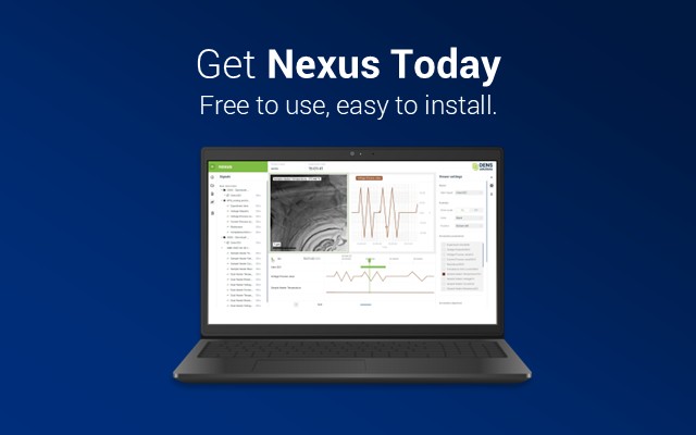
Looking for a simpler way to make sense of your in situ experiment data? Try our free in situ experiment data integration and visualization software, Nexus.

In situ electron microscopy experiments generate large and complex datasets over extended periods of time. As experiments become more dynamic and data-rich, extracting clear insights and maintaining context throughout the experiment can be challenging. We developed Nexus specifically to address this challenge. As a free data integration and visualization software, Nexus helps researchers synchronize, navigate and visualize their in situ experiment data in one intuitive platform.
1) Seamless data synchronization from multiple sources
Nexus enables the direct import of (S)TEM images and videos from platforms such as DigitalMicrograph®, Velox™, and TIA™, alongside stimuli logs from PSTrace™ and DENSsolutions’ Impulse™ software. All datasets are automatically aligned on a shared timeline, ensuring accurate temporal correlation across imaging and experimental conditions. By removing the need for manual timestamp matching, Nexus allows researchers to focus on interpreting how structural changes in the sample relate to applied stimuli.
Video 1: Screen recording demonstrating how to load different datasets in Nexus and subsequently synchronize them.
2) Effortless navigation of experiment timelines
(S)TEM in situ experiments often run for hours, generating extensive image, video, and stimuli datasets. Manually combing through this volume of data to pinpoint key moments of interest can be both time-consuming and frustrating. Nexus addresses this challenge with an intuitive, timeline-based interface that allows seamless, chronological browsing of your entire experiment.
Video 2: Screen recording highlighting Nexus’s intuitive navigation feature.
3) Integrated visualization of complex in situ datasets
Nexus brings multiple data streams together in powerful visualizations. Users can view images, videos, and stimuli data side by side, or in combined views that highlight relationships between structure and conditions. The software also supports annotations, measurements, scalebars and straightforward export of images, graphs and videos. This makes Nexus a practical tool not only for analysis, but also for preparing figures for publications, presentations and collaborative work.
Video 3: Screen recording showcasing the wide range of visualization and export options available in Nexus.
Get Nexus Today
Free to use, easy to install.


Sana Khalid | Cardiff University
“As a PhD student at Cardiff University, my research focuses on gas cell in situ STEM experiments, which involve running complex in-situ reactions using the Impulse system. After completing each experiment, it is crucial for me to synchronize the EMD data with the Impulse data to ensure accurate analysis and interpretation.
Nexus software has been incredibly helpful in streamlining this process. It allows me to easily integrate essential reaction parameters such as temperature, pressure, and gas flow rate, along with precise timestamps. This synchronization not only enhances the clarity and reliability of my data but also makes it far more presentable for publication and collaborative discussions.
Nexus has become an integral part of my workflow, and I highly recommend it to anyone working with in situ experiments.”
Get in touch
Do you have a question about any of our solutions and/or would you like to discuss your specific research needs? Share your details below, and we’ll be in touch soon.
Subscribe to our newsletter
Stay in the loop with the latest from DENSsolutions, from cutting-edge product launches to inspiring new in situ applications.