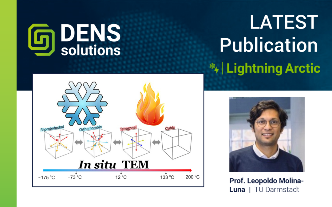
In situ TEM cooling meets high-precision heating: Exploring BaTiO₃ phase transitions with Lightning Arctic
Using the DENSsolutions Lightning Arctic system, researchers uncover the temperature-driven phase transitions and domain wall dynamics in single-crystal BaTiO₃ with atomic precision across cryogenic and elevated conditions.
Original article by Jiang et al.

Understanding the intricate phase transitions and domain dynamics of ferroelectric materials like barium titanate (BaTiO₃) is essential for improving their functional properties in applications such as capacitors, sensors and actuators. However, achieving atomic-resolution insights across a wide temperature range—spanning cryogenic to elevated conditions—remains a significant challenge. In a recent study published in Microstructures, Prof. Leopoldo Molina-Luna’s group at TU Darmstadt utilized our Lightning Arctic system to investigate the phase transitions and domain evolution of single-crystal BaTiO₃. By utilizing the system’s cryogenic cooling and heating capabilities, the team achieved unparalleled stability and resolution, enabling direct observations of phase behavior and domain wall dynamics from -175 °C all the way to 200 °C.
Lightning Arctic: Ultra-high stability
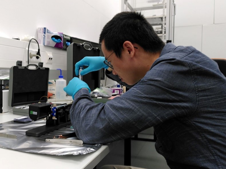
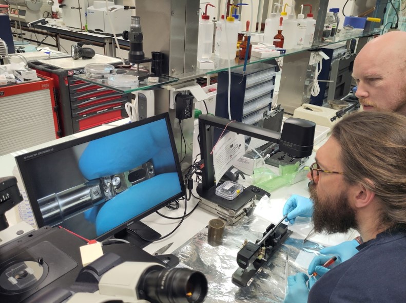
The DENSsolutions Lightning Arctic solution was used in this study for the application of in situ TEM cooling and heating. The cooling capability of Lightning Arctic is enabled via a cooling rod inside the holder, which transfers the ‘cold’ towards the holder’s tip where the MEMS-based Nano-Chip holding the sample is located. Once this cooling rod is connected to a metal cooling braid that is immersed in a liquid nitrogen dewar, the sample can be cooled inside the TEM to liquid nitrogen temperatures.
Impressively, the researchers were able to achieve atomic-resolution imaging at cryo-temperatures with notably low sample drift. This is due to the ultra-high stability of the holder. They captured a sequential of ten frames of HAADF STEM images on a single-crystal BTO TEM sample. The first frame, provided below in Figure 1a, evinces the exceptional stability of the holder, enabling atomic-resolution imaging at -175 °C.

Figure 1: Drift analysis in the cryo-STEM experiment at -175 °C.
Domain evolution during heating
Ferroelectric materials exhibit phase transitions that significantly influence their domain structures, which play a crucial role in determining material performance. By applying a controlled heating profile, the researchers were able to monitor how BaTiO₃ evolves through its various phases in real time. The video below highlights the dynamic changes in domain wall (DW) configurations as the material transitions from rhombohedral (R) to orthorhombic (O), tetragonal (T) and finally cubic (C) phases. At lower temperatures, zigzag patterns formed by 60° and 120° DWs appeared in the orthorhombic phase, while 90° a-c type ferroelastic domains became prominent in the tetragonal phase. These observations showcase how temperature influences domain behavior, offering valuable insights into the structural evolution of BaTiO₃ during heating.
Movie 1: Domain evolution during the complete in situ TEM heating process.
Domain evolution during cooling
Domain wall dynamics are central to understanding ferroelectric materials, as the movement and reorganization of these walls directly influence the material’s functional performance. Monitoring these processes in real time requires both exceptional resolution and imaging stability. The video below showcases the real-time evolution of domain walls across different temperature phases, enabled by the ultra-stable capabilities of the Lightning Arctic system. The researchers captured the movement and interaction of 71° and 180° DWs in the rhombohedral phase at cryogenic temperatures. These observations provide unprecedented clarity on the spontaneous strain and polarization mechanisms that govern domain stability, offering new insights into the nanoscale processes driving ferroelectric behavior.
Movie 2: Domain evolution during the complete in situ TEM cooling process.
Advancing the frontier of ferroelectric science
Conclusively, this study highlights the power of the DENSsolutions Lightning Arctic system in enabling atomic-resolution observations of phase transitions and domain wall dynamics in single-crystal BaTiO₃ across a wide temperature range. By capturing real-time structural evolution during both heating and cooling processes, Prof. Leopoldo Molina Luna and his group were able to reveal critical insights into the behavior of ferroelectric domains under temperature-driven stimuli. These findings lay the foundation for further studies of functional materials under multi-stimuli conditions, driving advancements in their development for next-generation applications.

“DENSsolutions’ Lightning Arctic enables in situ TEM of phase transitions with atomic precision.”
Prof. Leopoldo Molina-Luna | TU Darmstadt
Original article:
Discover our Lightning Arctic solution:

Lightning system helps uncover the interaction mechanism in reactive metal-ceramic system, Al-SiC
The DENSsolutions Lightning system was utilized to reveal the evolution mechanism of the Al–AOL–SiC system under heating and biasing conditions and under an ultrahigh resolution of 4 Å.