DENSsolutions partners with Bioz for AI-powered scientific search
We are thrilled to announce a significant enhancement to our website: the integration of the Bioz search engine – a cutting-edge tool empowering you to discover relevant publications with ease.
We recently integrated a state-of-the-art publications search tool, powered by cutting-edge artificial intelligence technology, across multiple pages on our website. Developed by Bioz, this innovative tool seamlessly scans through vast repositories of scientific papers, providing you with access to a wealth of information through sophisticated filtering capabilities.
Explore our new-and-improved Publications page
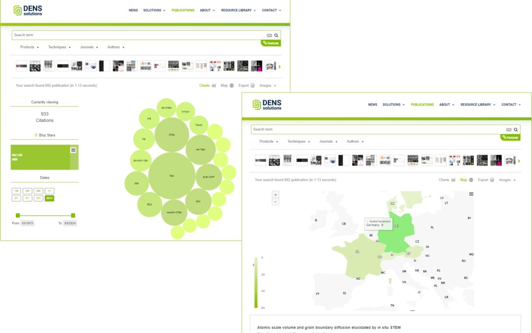
Previously, our Publications page allowed visitors to filter papers based solely on the type of DENSsolutions product used – namely Wildfire, Lightning, Climate or Stream. However, we understand that researchers appreciate more advanced search and filtering options to find tailored publications relevant to them. Therefore, we aimed to implement a tool on our website that would enable visitors to search for direct keywords applicable to their application or research focus. Moreover, a tool that would allow visitors to filter by the technique used, journal and even authors involved. This is precisely where Bioz comes in. You can now explore the tool on our updated Publications page. We would also like to highlight that with Bioz, you can make use of two unique features – the Charts and Maps feature. With Charts, you can visualize the popularity of all relevant techniques to in situ TEM, such as 4D-STEM, EELS and EDX. Moreover, the Maps feature allows you to see where all the authors of the papers are based.

Explore our updated product pages
Aside from the updates made to our Publications page, we’ve also revamped our product pages to allow for seamless searching of relevant publications as you acquaint yourself with each product. You can easily access these product pages through the links provided below. Note that as our latest solution Lightning Arctic was just launched some months ago, we plan to incorporate the Bioz platform directly into its dedicated webpage as publications begin to accumulate.


About Bioz
Bioz, an AI software company based in Silicon Valley, uses AI, machine learning and natural language processing in order to extract experimentation data from scientific articles. Bioz AI was developed by AI experts from Microsoft and Google, and with Nobel Prize winners in chemistry. The Bioz search engine offers researchers billions of data-driven product, technique and protocol recommendations. By harnessing the power of AI, Bioz provides researchers with an unprecedented amount of summarized scientific experimentation knowledge right at their fingertips. They are used by over 2 million researchers from over 17,000 different universities and companies in 196 countries. Their search engine is fueled with 300,000 million different products, 50,000 suppliers and 3,000 research techniques.
Visit our Publications page: