Study of microstructure of nickel-based superalloys at high temperatures
In Situ TEM Analysis of Organic–Inorganic Metal-Halide Perovskite Solar Cells under Electrical Bias
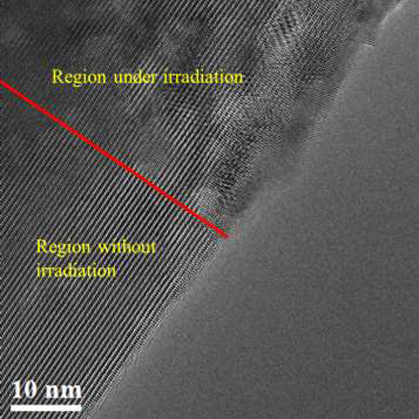
Atomic-Scale Observation of Irradiation-Induced Surface Oxidation by In Situ Transmission Electron Microscopy
