by Merijn Pen | Jul 10, 2017
Dr. Martial Duchamp
Ernst Ruska-Center for Microscopy and Spectroscopy with Electrons (ER-C) and Peter Grünberg Institute, Forschungszentrum, Jülich, Germany
Application |
Convenient Preparation of High-Quality Specimens for Annealing Experiments in the Transmission Electron Microscope |
Authors |
Martial Duchamp, Qiang Xu and Rafal E Dunin-Borkowski. |
Journal |
Microsc. Microanal. 2014, page 1 of 8 |
Publication |
Full Publication Here – DOI:10.1017/S1431927614013476 |
Convenient Preparation of High-Quality Specimens for Annealing Experiments in the Transmission Electron Microscope
ABSTRACT: A procedure based on focused ion beam milling and in situ lift-out is introduced for the preparation of high-quality specimens for in situ annealing experiments in the transmission electron microscope. The procedure allows an electron-transparent lamella to be cleaned directly on a heating chip using a low ion energy and back-side milling in order to minimize redeposition and damage. The approach is illustrated through the preparation of an Al–Mn–Fe complex metallic alloy specimen.
Figure left: Schematic diagram showing the configuration of an FEI dual-beam FIB Helios workstation with the α-flip (AF) holder mounted on the stage. The solid orange lines show the AF and tiltangles. The dotted orange line shows the total tilt angle of thespecimen compared with the horizontal. The inset shows a schematic diagram of a transmission electron microscopic lamella to define the terms used in the text. FIB, focused ion beam.
Figure above: a–i: Scanning electron microscopic images of the different steps used to transfer a 20103 μm lamella from bulk material to a double-tilt heater chip. The tilt angles, positions of the micro-manipulator and Pt needle, and the deposition and etching parameters are given in Table 1. The red arrows in (i) indicate ion-beam-deposited Pt (see text for details).
Figure above: a-c: Focused ion beam (FIB) and (d–f) scanning electron microscopic (SEM) images of the different thinning steps. The tilt angles and milling parameters are given in Table 1: (a) and (d) were acquired after transfer of the lamella onto the chip; (b) and (e) were acquired after milling at 81 pA (step 17 in Table 1); and (c) and (f) after milling at 47 pA (step 18 in Table 1); (g) bright-field; (h) dark-field; and (i) high-angle annular dark-field scanning transmission electron microscopic (STEM) images taken with the STEM detector of the FEI dual-beam Nanolab FIB Helios system. The scale bar for the FIB and SEM images is given in (f), while the scale bar of the STEM images is given in (i). The dot line in (a) shows the edge of the V shape created by the milling in steps 4 and 5 in Table 1, in this way the middle of the lamella can be found when using the back-side milling configuration during the thinning procedure.
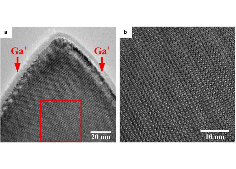
Figure left: High-resolution transmission electron microscopic images of the complex metallic alloy specimen attached to a DENSsolutions double-tilt heater chip for annealing experiments. a: Lower side of the lamella in the back-side milling configuration [exposed to the focused ion beam (FIB) during the thinning procedure]. b: Magnified area shown by the red box in (a), ∼50 nm from the specimen edge. The red arrows in (a) show the FIB milling direction.
by Merijn Pen | Jul 10, 2017
Application |
In Situ Atomic-Scale Observation of Electrochemical Delithiation Induced Structure Evolution of LiCoO2 Cathode in a Working All-Solid-State Battery |
Authors |
Yue Gong, Jienan Zhang, Liwei Jiang, Jin-An Shi, Qinghua Zhang, Zhenzhong Yang, Dongli Zou, Jiangyong Wang, Xiqian Yu, Ruijuan Xiao, Yong-Sheng Hu, Lin Gu , Hong Li, and Liquan Chen |
Journal |
J. Am. Chem. Soc., 2017, 139 (12), pp 4274–4277 |
Publication |
http://pubs.acs.org/doi/abs/10.1021/jacs.6b13344 |
In Situ Atomic-Scale Observation of Electrochemical Delithiation Induced Structure Evolution of LiCoO2 Cathode in a Working AllSolid-State Battery
ABSTRACT: We report a method for in situ atomic-scale observation of electrochemical delithiation in a working all-solid-state battery using a state-of-the-art chip based in situ transmission electron microscopy (TEM) holder and focused ion beam milling to prepare an all-solid-state lithium-ion battery sample. A battery consisting of LiCoO2 cathode, LLZO solid state electrolyte and gold anode was constructed, delithiated and observed in an aberration corrected scanning transmission electron microscope at atomic scale. We found that the pristine single crystal LiCoO2 became nanosized polycrystal connected by coherent twin boundaries and antiphase domain boundaries after high voltage delithiation. This is different from liquid electrolyte batteries, where a series of phase transitions take place at LiCoO2 cathode during delithiation. Both grain boundaries become more energy favorable along with extraction of lithium ions through theoretical calculation. We also proposed a lithium migration pathway before and after polycrystallization. This new methodology could stimulate atomic scale in situ scanning/TEM studies of battery materials and provide important mechanistic insight for designing better all-solidstate battery.
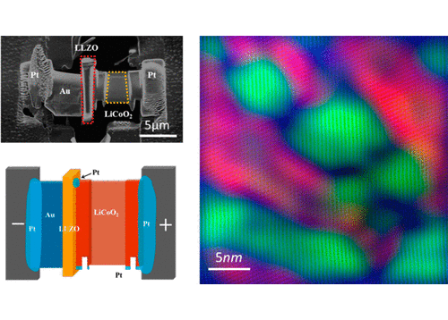
Figure left: (A) SEM image of the FIB fabricated battery on the nanochip to apply the electric field, and corresponding schematic (B). In panel A, the LLZO electrolyte and electron transparent area of the LiCoO2 cathode are highlighted with a red dashed line and a yellow dashed line trapezoid. Panels C and D are pristine LiCoO2 ABF and HAADF micrographs with the corresponding line profile acquired at the red dashed line rectangular zone shown in panel C with both lithium and oxygen contrast. In panels B and C, green, purple, and cyan balls are lithium, oxygen, and cobalt ions, respectively.