Breaking boundaries: Electrochemical impedance spectroscopy meets environmental TEM
Employing the DENSsolutions Lightning system, researchers were able to apply a novel integrated EIS-ETEM approach to a common ceramic electrolyte, subjecting it to an array of stimuli, such as reactive gases, elevated temperatures and applied electrical potentials.
Original article by Ma et al.

Preparing and conducting high-temperature solid-state electrochemical TEM – particularly relevant to solid oxide fuel and electrolysis cells (SOFC and SOEC) – poses a number of challenges. These challenges include ensuring mechanical stability during chip mounting, preventing sample fracture or loss of electrical contact and minimizing unavoidable leak currents through the chip components. Despite its many challenges, the integration of electrical impedance spectroscopy and environmental TEM uniquely facilitates the direct correlation between electrochemical activity and the nanoscale structure and composition of materials. In a recent paper published in Small Methods – involving our dear user at the Technical University of Denmark (DTU), Dr. Søren Bredmose Simonsen – the DENSsolutions Lightning system was utilized to study micro gadolinia-doped ceria (CGO). The behavior of CGO, a ceramic electrolyte with various electrochemical properties, was investigated under a diverse range of stimuli, including reactive gasses (O₂ and H₂/H₂O), elevated temperatures (room temperature — 800 °C) and applied electrical potentials. Importantly, this research marks a significant advancement in materials science, pioneering the integration of EIS with in situ ETEM.
CGO sample structure
Dr. Simonsen and his fellow collaborators meticulously designed the CGO sample for operando EIS-TEM investigations. A snapshot of the mounting process on the DENSsolutions Lightning Nano-Chip is shown in Figure 1b below. With a thin central part flanked by thick side parts, this sample configuration facilitates the separation of the contribution of bulk charge transport and the surface reaction processes. Notably, Dr. Simonsen emphasized the unique benefits of the Lightning Nano-Chip, highlighting its advantageous geometry. He explained, “The geometry of the DENSsolutions Lightning Nano-Chip is uniquely beneficial for our studies as it features a relatively long distance between the heater and the sample region. This allows us to mount and post-thin samples without the risk of creating pathways for leak current between the heater and sample or biasing electrodes.”

Figure 1: CGO sample mounted on a DENSsolutions Lightning Nano-Chip, visualized by SEM, TEM and HRTEM imaging.
EIS electrical circuit model
The researchers then explored the EIS spectra under three different gas environments at temperatures from 500 °C to 800 °C (see Figure 2 below). The Nyquist plots from EIS data reveal two distinct arcs, each representing different electrochemical processes. Through electrical circuit modeling, the contributions of resistances and capacitances are shown. Notably, the surface exchange reaction resistance exhibits a clear temperature dependence, reflecting thermally activated processes for both the transport and surface reaction.

Figure 2: EIS spectra (symbols) and fittings (lines) recorded in a) 3 mbar O₂ and in a H₂/H₂O with partial pressure ratio of b) 0.003 and c) 0.8; 10 kHz (square); 100 Hz (diamond), 1 Hz (circle), 0.1 Hz (triangle) are noted on the spectra, with hollow symbols.
Schematic illustration of CGO sample
In Figure 3 below, a schematic diagram of the differences for the CGO TEM sample in O₂ and H₂/H₂O is presented. Notably, in both O₂ and H₂/H₂O atmospheres, the conductivity and surface exchange reaction of CGO demonstrate notable dependencies on the gas environment. In the two scenarios, there are distinct chemical reaction formulas. In O₂, CGO predominantly conducts ions, confining the active surface near the Pt current collector. However, in the H₂/H₂O environment, electrons flow through CGO’s side parts, activating the entire surface.

Figure 3: Illustration of active surface area for Pt-CGO as a) pure ionic conductor and as b) mixed electronic/ionic conductor. Arrows indicate the direction of ions (red) and electrons (navy).
Electrochemical EIS meets TEM
The researchers then analyzed the transport and surface exchange resistance from the EIS measurements in each type of gas environment separately. Figure 4 below delves into the temperature and oxygen partial pressure (pO₂) dependence of CGO conductivity and surface exchange resistivity in different gas atmospheres. Notably, the conductivity in O₂ exhibits a characteristic temperature-dependent behavior, aligning closely with reference data for bulk polycrystalline CGO. Conversely, in H₂/H₂O environments, the conductivity shows a marked increase with decreasing oxygen partial pressure, indicative of a shift towards mixed electronic and ionic conduction. Moreover, the surface exchange resistance demonstrates a consistent decrease with increasing H₂/H₂O ratio, underscoring the influence of electronic charge carriers on electrochemical processes.

Figure 4: Electrochemical EIS-TEM measurements of CGO in different atmospheres via Arrhenius plots.
A novel integration
Dr. Simonsen and his fellow collaborators performed a comprehensive in situ TEM heating and biasing study using the DENSsolutions Lightning system, elucidating the nuanced interplay between gas environment, temperature and material properties of micro gadolinia-doped ceria, a common ceramic electrolyte. This innovative research taps into new academic frontiers by combining electrochemical impedance spectroscopy with in situ environmental transmission electron microscopy investigations. Importantly, the developed EIS-TEM platform in this study is an important tool in promoting the understanding of nanoscale processes for green energy technologies, such as solid oxide electrolysis/fuel cells, batteries, thermoelectric devices and many more.

“The geometry of the DENSsolutions Lightning Nano-Chip is uniquely beneficial for our studies as it features a relatively long distance between the heater and the sample region. This allows us to mount and post-thin samples without the risk of creating pathways for leak current between the heater and sample or biasing electrodes. Moreover, if not for the Lightning system’s low internal capacitance and high resistance, it would not have been possible to conduct electrochemical measurements for our materials.”
Dr. Søren Bredmose Simonsen Senior Research | Technical University Denmark
Original article:
Discover our Lightning solution:
Discover more publications made possible by Lightning:

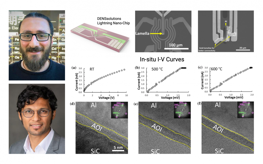
Lightning system helps uncover the interaction mechanism in reactive metal-ceramic system, Al-SiC
The DENSsolutions Lightning system was utilized to reveal the evolution mechanism of the Al–AOL–SiC system under heating and biasing conditions and under an ultrahigh resolution of 4 Å.